Project 1 - 40-V to 80-V adjustable output voltage boost reference design for LIDAR applications
Description: To design a non-synchronous boost controller to provide an adjustable output of between 40 V and 80 V capable of delivering a maximum of 100 mA of current to the load. This is an automotive design intended to power various applications such as LiDAR systems, which require an adjustable voltage supply.
Question:
- How will you decide the layer stack up.
Answer:
Layer stack-up means the arrangement of the copper layers and the insulating layers before PCB layout design, and these layers form a PCB. The consideration of layer stack-up depends on the technical capabilities of the production and the electrical performance requirements of the PCBs.
Stack-up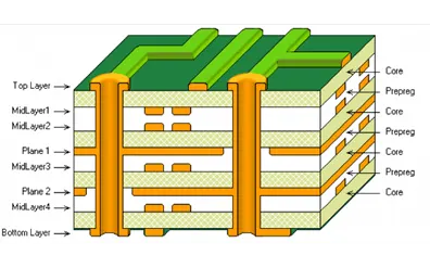 refers to the arrangement of copper layers and insulating layers that make up a PCB prior to board layout design. While a layer stack-up allows you to get more circuitry on a single board through the various PCB board layers, the structure of PCB stackup design confers many other advantages:
• A PCB layer stack can help you minimize your circuit's vulnerability to external noise as well as minimize radiation and reduce impedance and crosstalk concerns on high-speed PCB layouts.
• A good layer PCB stack-up can also help you balance your need for low-cost, efficient manufacturing methods with concerns about signal integrity issues.
To decide the layer stack up, consider the following factors:
· Layer Count
· Signal Integrity
· Power and Ground Planes
· Thermal Considerations
· EMI/EMC Considerations
· Material Selection
· Signal Layer Ordering
Generally, a higher number of layers can provide more routing space, better noise isolation, lower impedance, and higher reliability. However, it also increases the complexity, thickness, and cost of the board. For a non-synchronous boost controller, you may need at least four layers to accommodate the power and ground planes, the input and output traces, and the feedback and control signals.
- How do you calculate the trace width, via size and trace length.
Answer:
Trace width:
The trace width is calculated as follows:
First, the Area is calculated:
Area[mils^2] = (Current [Amps]/ (k*(Temp_Rise [deg. C]) ^b)) ^(1/c)
Then, the Width is calculated:
Width[mils] = Area[mils^2]/(Thickness[oz]*1.378[mils/oz])
For IPC-2221 internal layers: k = 0.024, b = 0.44, c = 0.725
For IPC-2221 external layers: k = 0.048, b = 0.44, c = 0.725
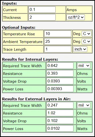
By using the above formula trace width calculated for internal layers is 0.642 mils and External layers 0.247 mils.
Via Size:
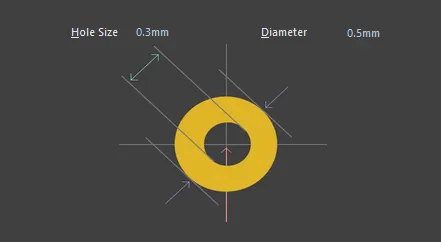
To calculate the size of a via, there are a few things to consider:
- Manufacturing cost: Opting for a larger via is going to carry lower manufacturing costs.
- Trace width: It’s generally accepted that the pad size should be somewhat larger than the via size.
- Reliability: Larger lands will be more reliable.
The IPC-2222 standard specifies minimum hole diameters for plated through-hole vias for different classes of vias :
- Minimum hole size = Maximum lead diameter + 0.25 mm (Level A)
- Minimum hole size = Maximum lead diameter + 0.20 mm (Level B)
- Minimum hole size = Maximum lead diameter + 0.15 mm (Level C)
The minimum via pad diameter can be calculated using the following equation:
L = a + 2b + c
Where:
a = Diameter of the finished hole (external layers) or diameter of the drill hole (internal layers)
b = Minimum annular ring size
c = Minimum standard fabrication allowance for interconnect lands.
Trace Width:
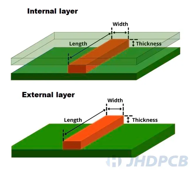
Any electronic signal requires a specific amount of time to travel through a conductor from its source to its destination. An electronic signal, whether digital or analog, travels along a trace with a velocity that equals the speed of light in the PCB substrate material. This speed, in turn, depends on the effective Dk value of the trace. The Dk value for the PCB substrate, the geometry of the trace, and the geometry of the conductor all determine the speed of signals in your traces.
The calculation method for PCB trace width depends on whether it is an internal or external trace. For internal traces, the following formula can be used:
w = (I * K * T)/(ΔT * A)
where:
w = trace width (in mils)
I = maximum current (in amps)
K = thermal conductivity of copper (385 W/mK)
T = trace thickness (in oz/ft^2)
ΔT = maximum temperature rise (in Celsius)
A = cross-sectional area of the trace (in mils^2)
For external traces, the following formula can be used:
w = (I * K * T)/(ΔT * (0.048 * (T + 100)))
where:
w = trace width (in mils)
I = maximum current (in amps)
K = thermal conductivity of copper (385 W/mK)
T = trace thickness (in oz/ft^2)
ΔT = maximum temperature rise (in Celsius)
- What is the drawback of having 2 layers PCB?
Answer:
- They have limited space for components and routing options, which can affect the performance and functionality of the circuit.
- They are more susceptible to crosstalk and noise, which can degrade the signal quality and reliability of the circuit.
- They have a higher weight and larger size, which can make them unsuitable for applications that require portability and miniaturization.
- They have a simplistic design, which can limit the features and capabilities of the circuit.
- It can also lead to signal integrity issues and electromagnetic interference (EMI).