Project 1
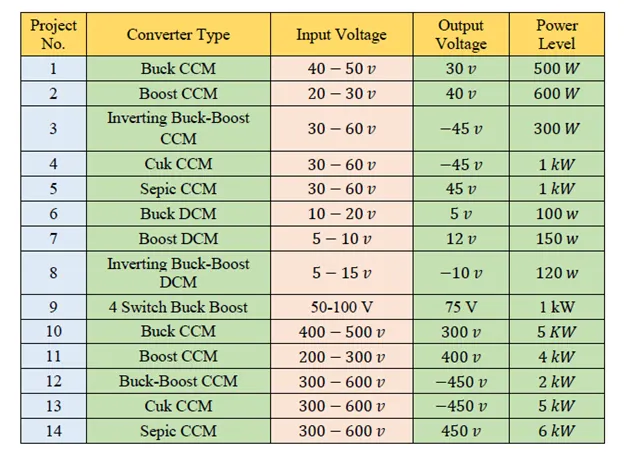
The project design report should include the following:
- A Design report to show the reasoning behind your choices of inductance and capacitance levels in your design.
- The full schematics of your converter including gate drivers, PWM chips, RC circuits, current sensors, voltage sensors, etc…
- A complete simulation file including all the necessary waveforms and justifying all the chosen components sizing (you have to show the system ability to track the output voltage at different dynamic conditions).
The full specs for all needed components in your circuits.
Note: Feel free to deviate from the provided specs as long as you are using the assigned converter. However, you cannot copy the specs of another assigned converter
Solution:
Three converters i.e., Buck converter, Boost converter and SEPIC converter are chosen for this project and the details of each converter along with its simulation results are discussed below.
MOSFET:
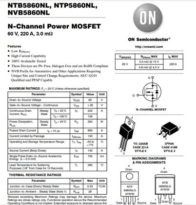
To make this simulation for industrial or practical application the MOSFET switch considered is NTB5860NL n channel power MOSFET. The specification of this MOSFET switch is given below.
- SEPIC CONVERTER
Input Voltage= 30-60V
Average Input Voltage= 45V
Output Voltage= 45V
Power = 1kW
Switching Frequency = 50 kHz
As per given data a SEPIC Converter can be used for the application.
Therefore, Duty cycle for SEPIC converter can be calculated as,
`V_o/V_s = D/(1-D)`
So,
On solving the above equation when Vs=45V, D= 0.5
Load resistance can be calculated as
`P_o= 〖V_o〗^2/R`
Po= 1kW
Vo= 45V
So, on solving for R,
R=2.025 ohm
Inductor Current can be calculated using
`I_L= (V_o I_0)/V_s`
`P_o= V_o I_o`
`I_o= P_o/V_o`
Io= 22.2A
So, on solving the above equation, IL= 22.2A
The variation in current is assumed as 10%, so = 2.22A
If the switching frequency is 50 kHz, then the inductance L1 for continuous current is determined from Equation,
`L_1=(V_s D)/(〖∆i〗_L1 f)`
`L_1=(45*0.5)/(2.22*50000)`
On solving the above equation,
L1= 2.02*10-4 H
For L2, the average current is determined from Kirchhoff’s current law at the node where C1, L2, and the diode are connected. The average current in each capacitor is zero, so the average current in L2 is
IL2=Io
IL2=2.22A
The variation in IL2 is determined from the circuit when the switch is closed. Using Kirchhoff’s voltage law around the path of the closed switch, C1, and L2 with the voltage across C1 assumed to be constant Vs. The minimum variation in current of 10 percent is determined from Equation,
`〖∆i〗_L1=22.2*0.1= 2.22 A`
`L_2=(V_s D)/(〖∆i〗_L2 f)`
`L_1=(45*0.5)/(2.22*50000)`
L1= 2.02*10-4 H
The output stage consisting of the diode, C2, and the load resistor is the same as in the boost converter, so the output ripple voltage and variation in capacitor C1 is assumed to be 10%.
`C_2≥D/(〖∆V〗_o/V_o R*f)`
On solving above equation, C2
`C_2≥49.4*10^(-6) F`
The voltage variation in C1 is determined from the circuit with the switch closed. Capacitor current iC1 is the opposite of iL2,
So,
`C_1≥D/(〖∆V〗_C1/V_o R*f)`
On solving the above equation C1= 49.4*10-6F
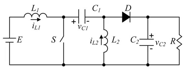
Schematic Diagram of SEPIC converter:
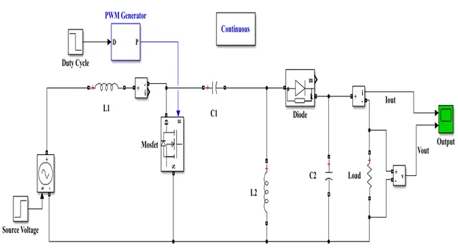
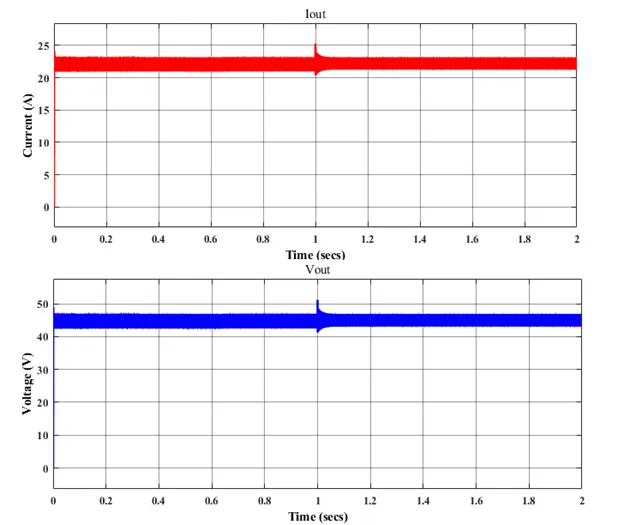
Simulation:
Zoom IN Simulation Result:
Output Voltage and Output Current:
Zoom OUT Simulation Result:
Output Voltage and Output Current:
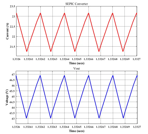
Result:
|
S.N |
Parameter |
Theoretical Result |
Simulation Result |
|
1. |
Source Voltage |
30-60V |
45-60V |
|
2. |
Average Voltage |
45V |
44.9V |
|
3. |
Switching Frequency |
50kW |
50kW |
|
4. |
Inductor, L1 |
2.02e-4H |
2.02e-4H |
|
5. |
Power |
999.67W |
1000W |
|
6. |
Inductor, L2 |
2.02e-4H |
2.02e-4H |
|
7. |
Capacitor, C1 and C2 |
49.4e-6F |
49.4e-6F |
|
8. |
Load Resistance |
2.025 ohm |
2.025 ohm |
|
9. |
Duty Cycle |
0.6>D>0.428 |
0.5>D>0.428 |
|
10. |
Output Voltage |
45V |
44.9V |
|
11. |
Output Current |
22.2A |
22.2A |
Conclusion: SEPIC converter is designed as per given data and result obtained through simulation proves theoretical result.
2. BOOST CONVERTER
Input Voltage= 20-30V
Average Input Voltage= 25V
Output Voltage= 40V
Power = 600W
Switching Frequency = 50 kHz
As per the given data, a Boost Converter can be used for the application.
Therefore, Duty cycle for Boost converter can be calculated as,
`V_o/V_s = 1/(1-D)`
So,
`1-V_s/V_o = D`
On solving the above equation when Vs=25V, D= 0.375
Load resistance can be calculated as
`P_o= 〖V_o〗^2/R`
Po= 600W
Vo= 40V
So, on solving for R,
R=2.67 ohm
Inductor Current can be calculated using
`I_L= 〖V_o〗^2/(V_s*R)`
So, on solving the above equation, IL= 23.97A
If the switching frequency is 50 kHz, then the minimum inductance for continuous current is determined from Equation,
`L_min=(〖D(1-D)〗^2*R)/2f`
On solving the above equation,
Lmin= 3.91*10-6 H
A boost converter designed for continuous-current operation will have an inductor value greater than Lmin,
To provide a margin to ensure continuous current, let L= 5*10-6H
The minimum capacitance required to limit the output ripple voltage to 10 percent is determined from Equation,
`C≥D/(〖∆V〗_o/V_o R*f)`
`C≥56.18*10^(-6) F`
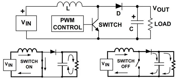
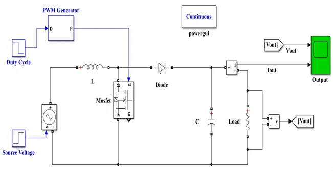
Schematic Diagram of Boost Converter:
Simulation
Zoom IN Simulation Result:
Output Voltage and Output Current:
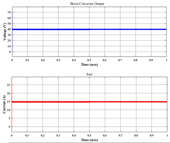
Zoom OUT Simulation Result:
Output Voltage and Output Current:
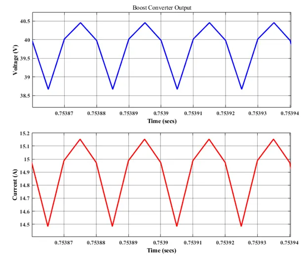
|
S.N |
Parameter |
Theoretical Result |
Simulation Result |
|
1. |
Source Voltage |
20-30 |
25-30 |
|
2. |
Duty Cycle |
0.5>D>0.25 |
0.375>D>0.25 |
|
3. |
Switching Frequency |
50kW |
50kW |
|
4. |
Average Voltage |
25V |
25V |
|
5. |
Inductor, L |
3.91e-6H |
5e-6H |
|
6. |
Power |
600W |
594.51W |
|
7. |
Capacitor, C |
56.18e-6F |
56.18e-6F |
|
8. |
Load Resistance |
2.67 ohm |
2.69 ohm |
|
9. |
Output Voltage |
40V |
39.9V |
|
10. |
Output Current |
15A |
14.9A |
Conclusion: Boost converter is designed as per given data and result obtained through simulation proves theoretical result.
3. BUCK CONVERTER
Given,
Input voltage= 40-50V
Output Voltage= 30V
Power = 500 W
Assuming Switching Frequency to be 50 kHz and input voltage to be 45V
We know that,
Duty cycle D, = Vout/ Vin
So D= 30/45
D= 0.66 or Duty cycle is 66%
Resistance R= (Vout)2/Po
R= (30)2/500 =1.8 ohms
Let us design for 10% ripple in the inductor
The switching frequency and inductor size must be selected for continuous-current operation. Let the switching frequency arbitrarily be 50 kHz, which is well above the audio range and is low enough to keep switching losses small. The minimum inductor size is determined from Equation:
So
`L_min= ((1-D)R)/〖2f〗_s`
`L= (1-0.66)1.8/(50000*2)`
`L= 6.12μH`
Let the inductor be 25 percent larger than the minimum to ensure that inductor current is continuous.
`L_min= 1.25*6.12μH`
`L= 7.65μH`
Capacitor Designing
The output voltage ripple is 5% assumed,
`C_out= ((1-D))/(8L*〖f_s〗^2* 〖δV〗_o/V_o )`
`C_out= ((1-0.66))/(8*7.65*10^(-6)*〖(50k)〗^2* 0.05)`
On solving, we get,
`C_out= 45 μF`
Schematic Diagram of Buck Converter:
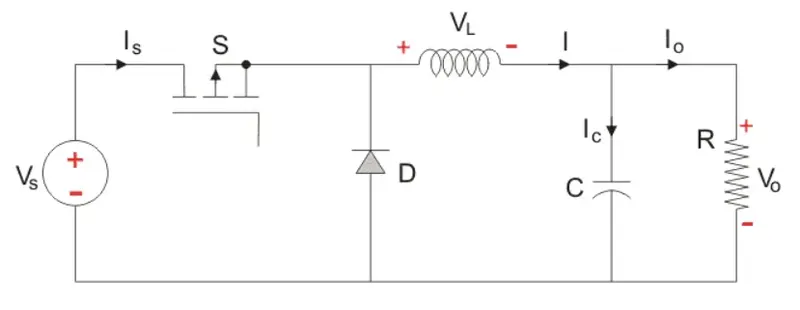
Simulation:
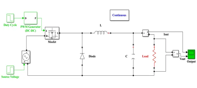
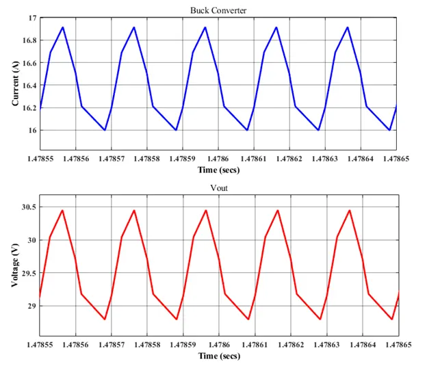
Zoom In Simulation Result:
Output Voltage and Input Voltage:
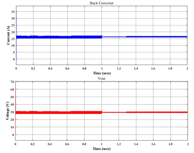
Zoom OUT Simulation Result:
Output Voltage and Output Current:
|
S.N |
Parameter |
Theoretical Result |
Simulation Result |
|
1. |
Source Voltage |
40-50 |
45-50 |
|
2. |
Duty Cycle |
0.5>D>0.25 |
0.375>D>0.25 |
|
3. |
Switching Frequency |
50kW |
50kW |
|
4. |
Average Voltage |
45V |
45V |
|
5. |
Inductor, L |
6.1e-6H |
7.65e-6H |
|
6. |
Power |
500W |
495.15W |
|
7. |
Capacitor, C |
45e-6F |
45e-6F |
|
8. |
Load Resistance |
1.8 ohm |
1.83 ohm |
|
9. |
Output Voltage |
30V |
30.1V |
|
10. |
Output Current |
16.67A |
16.45A |
Conclusion: Buck converter is designed as per given data and result obtained through simulation proves theoretical result.