Project 1
********************************BUCK CONVERTER *****************************
Design of Buck Converter:
Input voltage: 40V - 50V
Output Voltage : 30V
Power : 500W
Load Current: I = P/V = 500/30 = 16.67A
Load Resistor : Vo/Io = 30/16.67 =1.8 ohms.
1) schematic of the DC/DC converter:
Buck Converter:
2) Duty ratio of the converter.
Converter Ratio:
Dmin= Vo/Vin = 30/50 = 0.6.
Dmax = 30/40 = 0.75.
3) switching frequency of the converter:
The Switching Frequency of mosfet can go upto greater than 20kHz(Nominal). MOSFET has low switching losses. Whereever require circuit with low space constrain can move greater frequency to reduce the size of inductor and capacitor. For our design, Let choose Fsw = 20kHz.
4) Inductor Design:
Design Constrain:
1) Output current is continuous
2) inductor current ripple is less than 30%
In buck converter, Average Inductor current will equals to Load current.
IL = Iind
Delta Iind < 0.3*Iload;
Delta_Iind < 0.3*16.67 = 5A
For Continuous Output current: Lmin>= (1-D)R/(2*Fs)
Lmin @ D = 0.75
Lmin >= (1-0.75)*1.8/(2*20k)
Lmin >= 11.25uH
Lmin @ D = 0.6
Lmin >= (1-0.6)*1.8/(2*20k)
Lmin >= 18uH
The inductance required to maintain the CCM in all range of duty ratio should be greater 18uH.
Calculation of Inductor:
inductor current ripple is less than 30%:
L @ D = 0.75
L = Vo(1-D)/(Fs*Delta_Iind);
L = 30*0.25/(20k*5);
L = 75uH
Lmin @ D = 0.6
L = Vo(1-D)/(Fs*Delta_Iind);
L = 30*0.4/(20k*5);
L = 120uH
For maintaining 30% of ripple output current for all range of Duty ratio, The minimum inductance required 120uH.
5) Design of Output capacitor :
Design Constrain:
1) Output Voltage ripple is less than 5%
Delta_Vo = 0.05*Vo = 0.05*30 = 1.5V
Capacitor Cout = 1-D *Vo /(8*L*Fs^2*Delta_Vo)
Cout = 0.25*30/( 8*75u*20k*20k*1.5)
Cout = 20uF
The minimum Capacitance required to maintain 5% of ripple output Voltage in all range of duty ratio should be 20uF.
As Finalized, to maintain 10% ripple of current and 5% of Voltage ripple for all worst case conditions, the selection of Inductor and Capacitor as follows:
L = 120uH
C = 20uF
Results and Discussion:
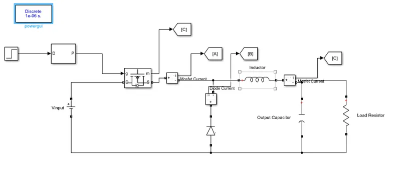
Case 1: Vin = 40V and D= 0.75
The Input Voltage is 40V and Duty ratio is 0.75 and buck converter are simulated and its output voltage and current, input voltage and current are shown below:
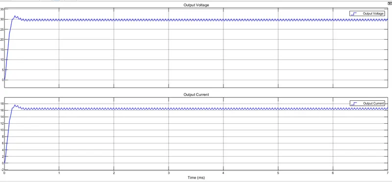
1) a) Output Voltage and Output Current:
The output voltage reaches the steady state is around .3ms. the transient peak voltage is around 32V peak.
The output voltage obtained is around 30V and Voltage ripple of1V(Peak to peak) which is less than calculated.
The average output current is around 16.7A.
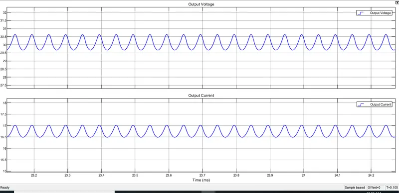
1) b) Output Voltage and Output Current:
Output Voltage and Output Current are shown in Zoom in Version.
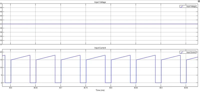
1) c) Input Voltage and Input Current:
Input volatge applied is 40V and the Peak Input current is around17A.
Case 2: Vin = 50V and D = 0.6
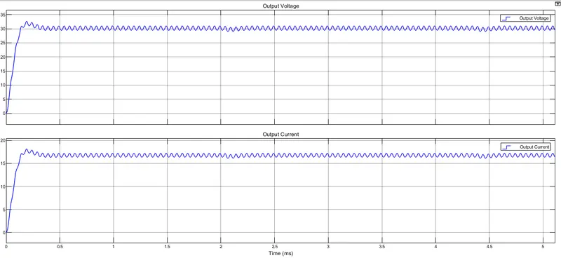
2) a) Output Voltage and Output Current:
The output voltage reaches the steady state is around 0.5ms. the transient peak voltage is around32V peak.
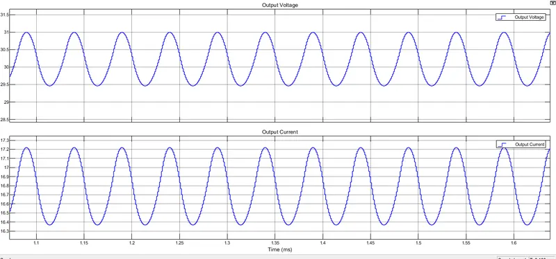
The output voltage obtained is around 30V and Voltage ripple of 1.5V(Peak to peak).
The average output current is around 16.8A.
2) b) Output Voltage and Output Current:
Output Voltage and Output Current are shown in Zoom in Version.
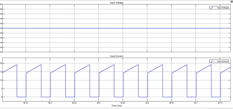
2) c) : Input Voltage and Input Current:
Input voltage applied is50V and the Peak Input current is around 17.3A.
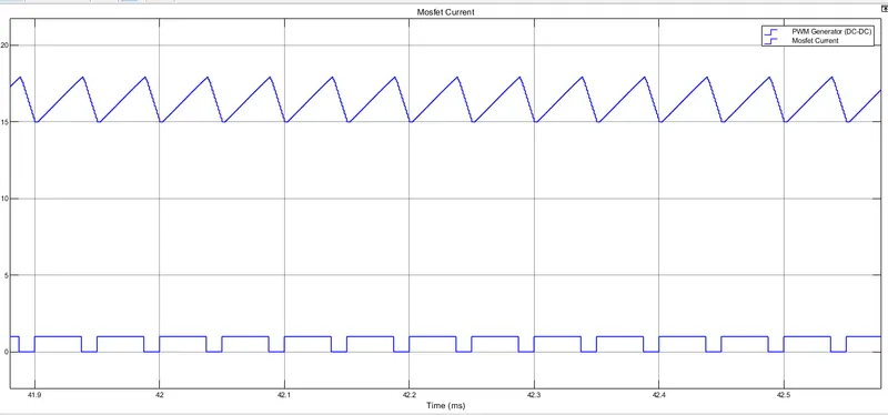
3) Inductor Current vs PWM Signal:
The PWM signal is applied to Gate driver of MOSFET and compared with inductor current waveform.
As we see, when MOSFET is ON, Inductor charges and Discharges when MOSFET is OFF condition. the circuit is simulated in CCM mode so that inductor current is not getting zero before the MOSFET is turned OFF. Inductor Current is continuous in nature.
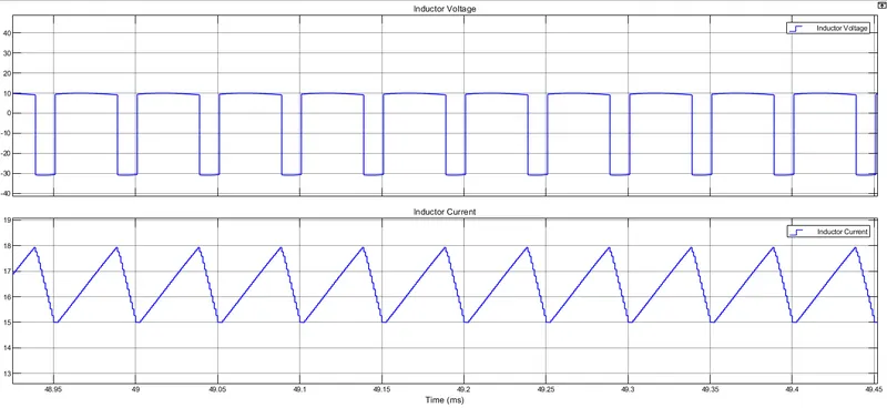
4) Inductor Voltage and Inductor Current:
The Inductor Voltage and Inductor current waveforms are simulated as shown. The inductor voltage swings between -30V to 10V as the input is 40V.
The average inductor current when the input voltage as 40V provided is around 17A with ripple peak to peak as 3A.
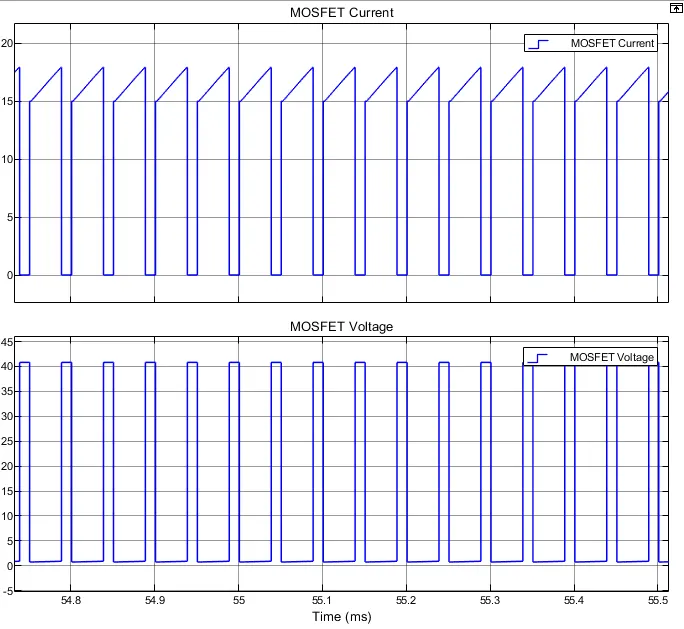
5) MOSFET Voltage and MOSFET Current:
When mosfet turn ON, Voltage across the mosfet gets Zero (small mill volts drop appears due to RdsON). In this case, we get 42V as Peak Mosfet voltage.
The MOSFET current increases suddenly to 15A when Switch turns ON. after turns ON the current gradually increases to approx. 17.6A.
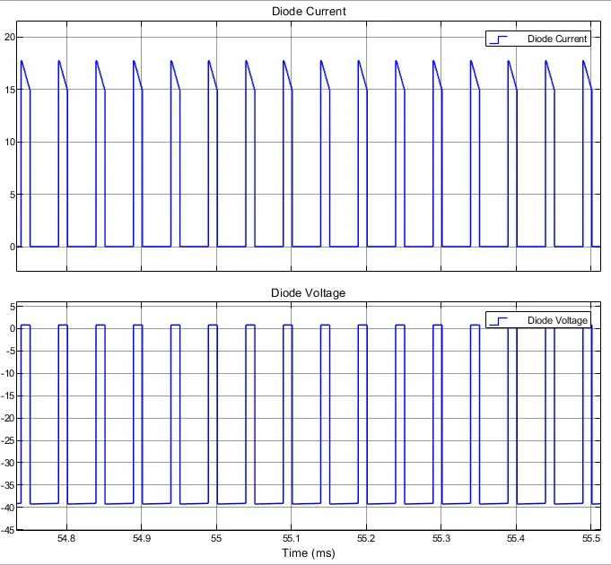
6) Diode Voltage and Diode Current:
when Diode turn ON, Voltage across the Diode will be equal to Forward Volatge drop (0.8V). When turns OFF, Peak diode Voltage is around -40V.
The DIODE current starts to conduct when MOSFET turns off to 17A when Switch turns ON. after turns ON the current gradually decreases to approx. 15A.
7) Efficiency
the efficiency of the converter will be calculated by following formula:
η = Power output/ Power input.
η = 495.3/574.1 = 86.27%
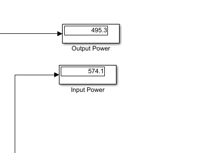
The efficiency was calculated includingg the MOSFET Resistance and Diode Forward drop and not including the Inductor and capacitor Resistance.
*****************************************************BOOST CONVERTER *********************************************************
Design of Boost Converter:
Input Data;
Vin =20 to 30 V
Vout =40V
Pout =600W
Fs = 100khz
calculate other unkowns:
Iout = Pout/Vout = 600/40 =15A
R(load) Vout/Iout = 40/15 = 2.667 ohms
DeltaVout = 5%*40V = 2V
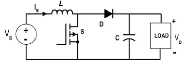
Draw a schematic diagram that you suggest them to use in this application:
The schematic diagram of Boost converter is shown below:
Duty ratio range of the converter.
we know that Vout = Vin/(1-D).
by solving Vin =20V , D= 1-(Vin/Vout) = 0.5
Vin = 30V , D = 1-(Vin/Vout) = 0.25
Design the switching inductor
let design the inductor with continuous conduction with Vin = 20V(worst case).
For CCM L>Lmin.
Lmin = D(1-D)^2*R/(2Fs)
by solving we get, Lmin = 1.7uH
To operate the converter in CCM, inductance of input filter must be greater than 2uH.
Let us take inductor current ripple to be 10%, and solve for inductance:
L = Vin*D/(Fs*deltaI)
Il = Input = Iout/(1-D) = 15/(1-0.5) =30A
Il = Input = Iout/(1-D) = 15/(1-0.25) =20A
deltaI = 10%*30 = 3A
deltaI = 10%*20 = 2A
By solving the above inductor equation we get
L = 33.33uH when Vin =20V @D = 0.5
L = 37.5uH when Vin =30V @D = 0.25
For maintaining 10% of ripple output current for all range of Duty ratio, The minimum inductance required 35uH.
Design an output capacitor such that the output voltage ripple is less than 5 %:
DeltaV = 2V
the output capacitance can be found by Cout = Vout*D/(R*Fs*DeltaV)
By solving Cout will be : Cout = 37uF
The minimum Capacitance required to maintain 5% of ripple output Voltage in all range of duty ratio should be 37uF.
As Finalized, to maintain 10% ripple of current and 5% of Voltage ripple for all worst case conditions, the selection of Inductor and Capacitor as follows:
L = 37.5uH
C = 37uF
Results and Discussion:
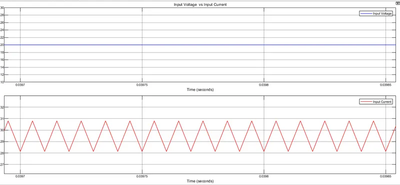
Case 1: Vin = 200V and D= 0.5
The Input Voltage is 200V and Duty ratio is 0.5 and boost converter are simulated and its output voltage and current, input voltage and current are shown below:
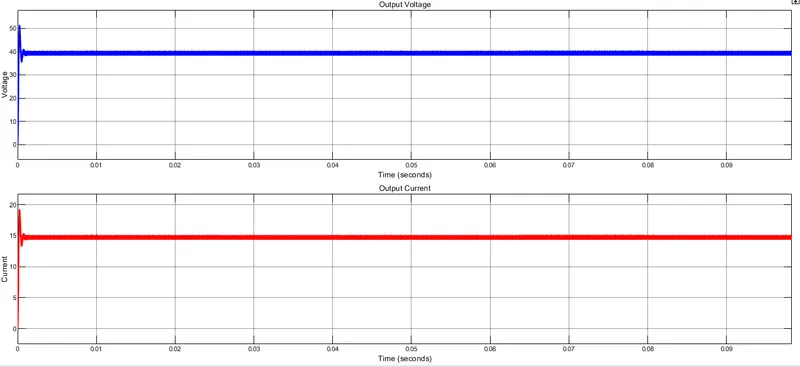
1) a) Output Voltage and Output Current:
The output voltage reaches the steady state is around 3ms. the transient peak voltage is around 700V peak.
The output voltage obtained is around 400V and Voltage ripple of 2V(Peak to peak) which is less than calculated.
The average output current is around 10A.
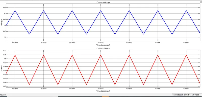
1) b) Output Voltage and Output Current:
Output Voltage and Output Current are shown in Zoom in Version.
1) c) Input Voltage and Input Current:
Input volatge applied is 200V and the average Input current is around 20A.
As in the boost converter, we know that Input current is equal to inductor current. the peak to peak ripple current of inductor is around 3A.
Case 2: Vin = 300V and D = 0.25
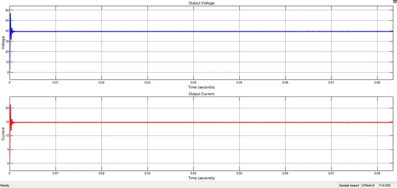
2) a) Output Voltage and Output Current:
The output voltage reaches the steady state is around 3ms. the transient peak voltage is around 700V peak.
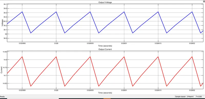
The output voltage obtained is around 396V and Voltage ripple of 1V(Peak to peak) which is less than calculated.
The average output current is around 9.95A.
2) b) Output Voltage and Output Current:
Output Voltage and Output Current are shown in Zoom in Version.
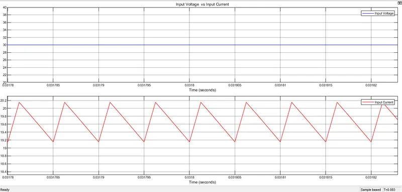
2) c) : Input Voltage and Input Current:
Input volatge applied is 300V and the average Input current is around 13.5A.
The peak to peak ripple current of input is around 1.3A.
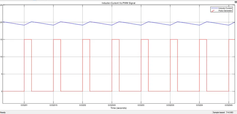
3) Inductor Current vs PWM Signal:
The PWM signal is applied to Gate driver of MOSFET and compared with inductor current waveform.
As we see, when MOSFET is ON, Inductor charges and Discharges when MOSFET is OFF condition. the circuit is simulated in CCM mode so that inductor current is not getting zero before the MOSFET is turned OFF. Inductor Current is continuous in nature.
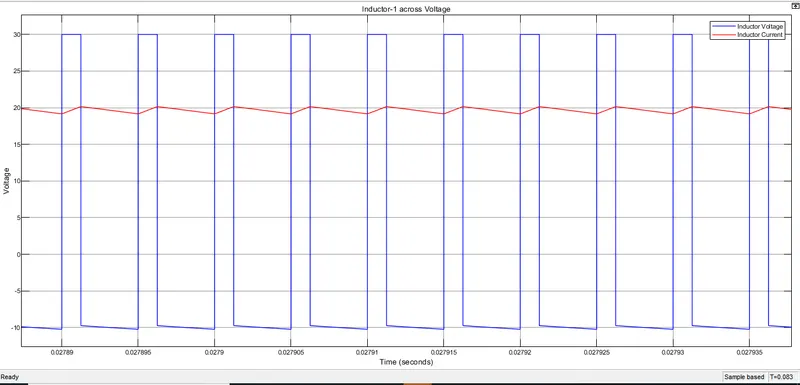
4) Inductor Voltage and Inductor Current:
The Inductor Voltage and Inductor current waveforms are simulated as shown. The inductor voltage swings between -200V to 200V as the input is 200V.
The average inductor current when the input voltage as 200V provided is around 20A with ripple peak to peak as 3A.
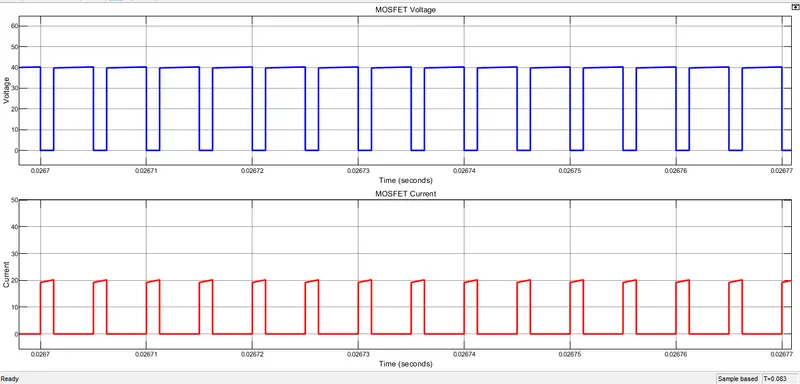
5) MOSFET Voltage and MOSFET Current:
When mosfet turn ON, Voltage across the mosfet gets Zero (small mill volts drop appears due to RdsON). When turns OFF, Voltage across the mosfet will be Inductor voltage + output voltage. In this case, we get 400V as Peak Mosfet voltage.
The MOSFET current increases suddenly to 20A(inductor current) when Switch turns ON. after turns ON the current gradually increases to approx. 22A.
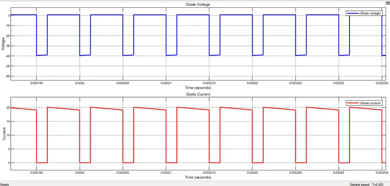
6) Diode Voltage and Diode Current:
when Diode turn ON, Voltage across the Diode will be equal to Forward Volatge drop (0.8V). When turns OFF, Peak diode Voltage is around -400V.
The DIODE current starts to conduct when MOSFET turns off to 20A(inductor current) when Switch turns ON. after turns ON the current gradually decreases to approx. 19A.
7) Efficiency
the efficiency of the converter will be calculated by following formula:
η = Power output/ Power input.
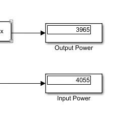
η = 3965/4055 = 97.7%
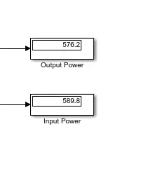
The efficiency was calculated includingg the MOSFET Resistance and Diode Forward drop and not including the Inductor and capacitor Resistance.
*****************************************BOOST CONVERTER******************************************************************
Design of Boost Converter:
Input Data;
Vin =200 to 300 V
Vout =400V
Pout =4000W
Fs = 200khz
calculate other unkowns:
Iout = Pout/Vout =4000/400 =10A
R(load) Vout/Iout = 400/10 = 40 ohms
DeltaVout = 2%*400V = 8V
Duty ratio range of the converter.
we know that Vout = Vin/(1-D).
by solving Vin =200V , D= 1-(Vin/Vout) = 0.5
Vin = 300V , D = 1-(Vin/Vout) = 0.25
Design the switching inductor
let design the inductor with continuous conduction with Vin = 20V(worst case).
For CCM L>Lmin.
Lmin = D(1-D)^2*R/(2Fs)
by solving we get, Lmin = 12uH
To operate the converter in CCM, inductance of input filter must be greater than 12uH.
Let us take inductor current ripple to be 10%, and solve for inductance:
L = Vin*D/(Fs*deltaI)
Il = Input = Iout/(1-D) = 10/(1-0.5) =20A
Il = Input = Iout/(1-D) = 10/(1-0.25) =13.33A
deltaI = 10%*20 = 2A
deltaI = 10%*13.33 = 1.33A
By solving the above inductor equation we get
L = 166.7uH when Vin =200V @D = 0.5
L = 282uH when Vin =300V @D = 0.25
For maintaining 10% of ripple output current for all range of Duty ratio, The minimum inductance required 282uH.
Design an output capacitor such that the output voltage ripple is less than 5 %:
DeltaV = 8V
the output capacitance can be found by Cout = Vout*D/(R*Fs*DeltaV)
By solving Cout will be : Cout = 12.5uF
The minimum Capacitance required to maintain 5% of ripple output Voltage in all range of duty ratio should be 12.5uF.
As Finalized, to maintain 10% ripple of current and 5% of Voltage ripple for all worst case conditions, the selection of Inductor and Capacitor as follows:
L = 282uH
C = 12.5uF
Results and Discussion:
Schematic of Boost converter:
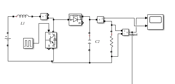
Case 1: Vin = 200V and D= 0.5
The Input Voltage is 200V and Duty ratio is 0.5 and boost converter are simulated and its output voltage and current, input voltage and current are shown below:
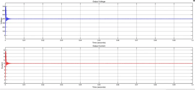
1) a) Output Voltage and Output Current:
The output voltage reaches the steady state is around 3ms. the transient peak voltage is around 700V peak.
The output voltage obtained is around 400V and Voltage ripple of 2V(Peak to peak) which is less than calculated.
The average output current is around 10A.
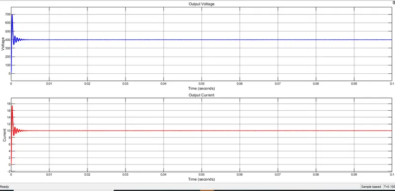
1) b) Output Voltage and Output Current:
Output Voltage and Output Current are shown in Zoom in Version.
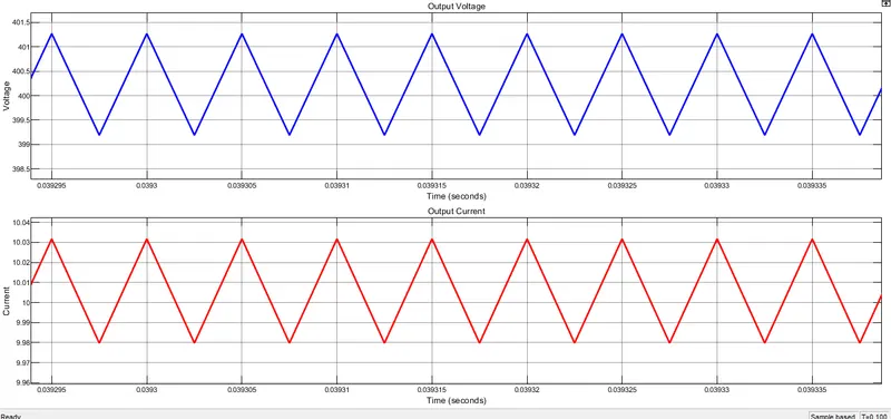
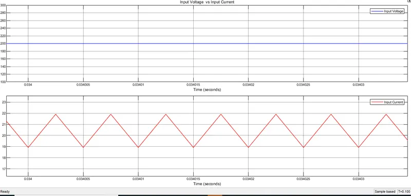
1) c) Input Voltage and Input Current:
Input volatge applied is 200V and the average Input current is around 20A.
As in the boost converter, we know that Input current is equal to inductor current. the peak to peak ripple current of inductor is around 3A.
Case 2: Vin = 300V and D = 0.25
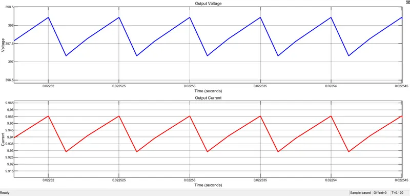
2) a) Output Voltage and Output Current:
The output voltage reaches the steady state is around 3ms. the transient peak voltage is around 700V peak.
The output voltage obtained is around 396V and Voltage ripple of 1V(Peak to peak) which is less than calculated.
The average output current is around 9.95A.
2) b) Output Voltage and Output Current:
Output Voltage and Output Current are shown in Zoom in Version.
2) c) : Input Voltage and Input Current:
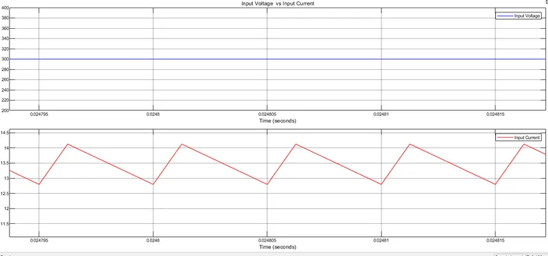
Input volatge applied is 300V and the average Input current is around 13.5A.
The peak to peak ripple current of input is around 1.3A.
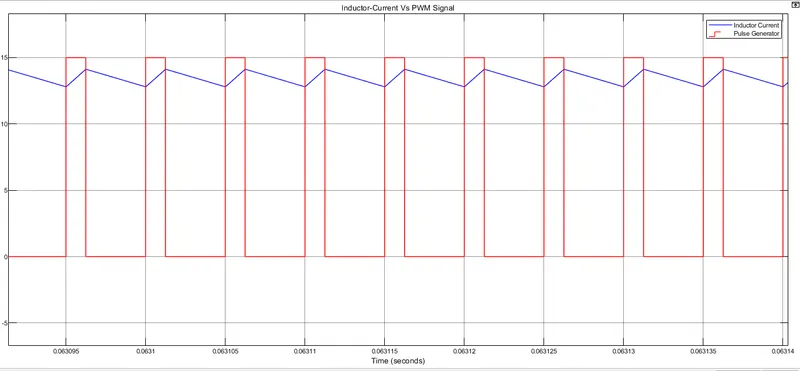
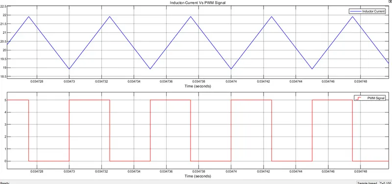
3) Inductor Current vs PWM Signal:
The PWM signal is applied to Gate driver of MOSFET and compared with inductor current waveform.
As we see, when MOSFET is ON, Inductor charges and Discharges when MOSFET is OFF condition. the circuit is simulated in CCM mode so that inductor current is not getting zero before the MOSFET is turned OFF. Inductor Current is continuous in nature.
4) Inductor Voltage and Inductor Current:
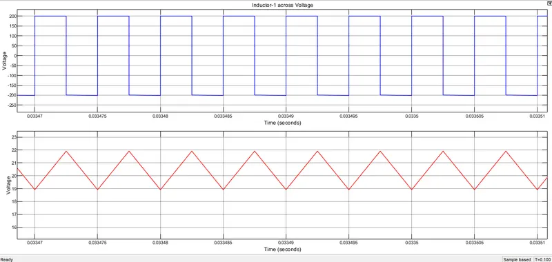
The Inductor Voltage and Inductor current waveforms are simulated as shown. The inductor voltage swings between -200V to 200V as the input is 200V.
The average inductor current when the input voltage as 200V provided is around 20A with ripple peak to peak as 3A.
5) MOSFET Voltage and MOSFET Current:
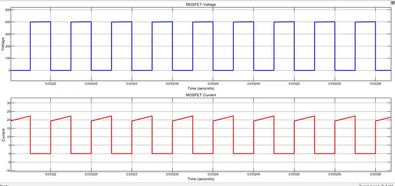
When mosfet turn ON, Voltage across the mosfet gets Zero (small mill volts drop appears due to RdsON). When turns OFF, Voltage across the mosfet will be Inductor voltage + output voltage. In this case, we get 400V as Peak Mosfet voltage.
The MOSFET current increases suddenly to 20A(inductor current) when Switch turns ON. after turns ON the current gradually increases to approx. 22A.
6) Diode Voltage and Diode Current:
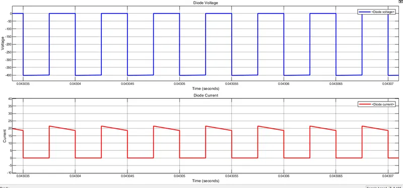
when Diode turn ON, Voltage across the Diode will be equal to Forward Volatge drop (0.8V). When turns OFF, Peak diode Voltage is around -400V.
The DIODE current starts to conduct when MOSFET turns off to 20A(inductor current) when Switch turns ON. after turns ON the current gradually decreases to approx. 19A.
7) Efficiency
the efficiency of the converter will be calculated by following formula:
η = Power output/ Power input.
η = 3965/4055 = 97.7%
The efficiency was calculated includingg the MOSFET Resistance and Diode Forward drop and not including the Inductor and capacitor Resistance.