Loss calculation for a DC/DC converter using MATLAB Simulink
Aim:
Design of boost converter, calculating the loss of different components including power switching device, and deriving efficiency of a boost converter. This is applicable in the power supply industry, electric vehicles, etc, where a DC-DC converter is required to boost the voltage from the DC source. All the aspects of this project with loss calculation, device selection, simulation, etc are industry-relevant.
Theory:
Boost Converter or Step-up Converter in CCM:
A boost converter is a type of DC-DC power converter that is used to step up a DC voltage from a lower level to a higher level. It is also known as a step-up converter.
In this converter, Inductor placed at the input side and switch(MOSFET, IGBT and BJT, etc.) is placed at the mid-side of the converter, we can see in the following figure-02;
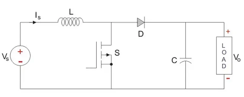
Figure <!-- [if supportFields]> SEQ Figure \* ARABIC <![endif]-->1<!-- [if supportFields]><![endif]-->- Conventional Boost Converter
Output Capacitor is used for to reduce the ripple in output voltage and make it constant at steady-state.
Diode is used to freewheel the energy of converter Inductor when the switch is OFF.
Basic Design Parameters:
Vin = 200-300V
Vout = 400V
Power = 4KW
Working Principle:
Since, a Boost converter contain non-linear devices such as one Switch and one uncontrolled Diode, hence the circuit operates in two mode as given below;
ON-Mode of Operation:
ON mode means the Switch is “ON” and the Diode is “OFF”. When we apply this the change in circuit as following;
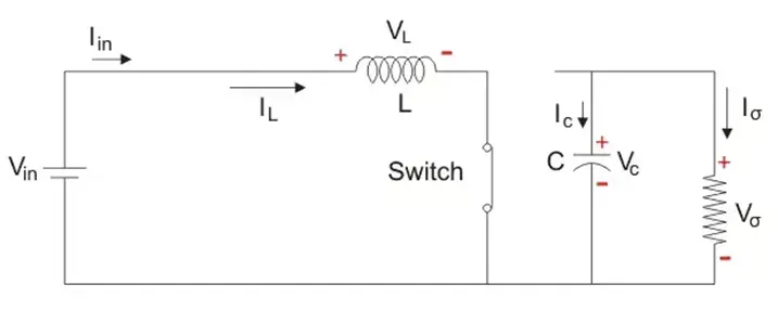
Figure <!-- [if supportFields]> SEQ Figure \* ARABIC <![endif]-->2<!-- [if supportFields]><![endif]-->- Boost converter during 'ON' Mode
During “ON” mode, DC voltage source deliver the energy to the inductor and inductor is linearly charged till the switch is in “ON” condition.
OFF-Mode of Operation:
OFF mode means the Switch is “OFF” and the Diode is “ON”. When we apply this the change in circuit as following;
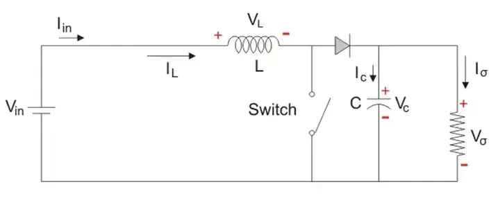
Figure <!-- [if supportFields]> SEQ Figure \* ARABIC <![endif]-->3<!-- [if supportFields]><![endif]-->- Boost converter during 'OFF' Mode
During “OFF” mode, freewheeling diode is activated and Inductor discharge energy through this path where this freewheeling diode is present.
Thus, we see that Converter inductor is charged during “ON” and discharge during “OFF” condition, so we observe that the waveform of the Inductor current is periodic, and we know very well that “If we passing periodic current through the Inductor than, the average Voltage across the Inductor should be zero”
Specs of Boost Converter in CCM:
Given,
Vin = (200-300)V,
Vout = 400V,
Power = 4KW,
Let, fs = 50KHz,
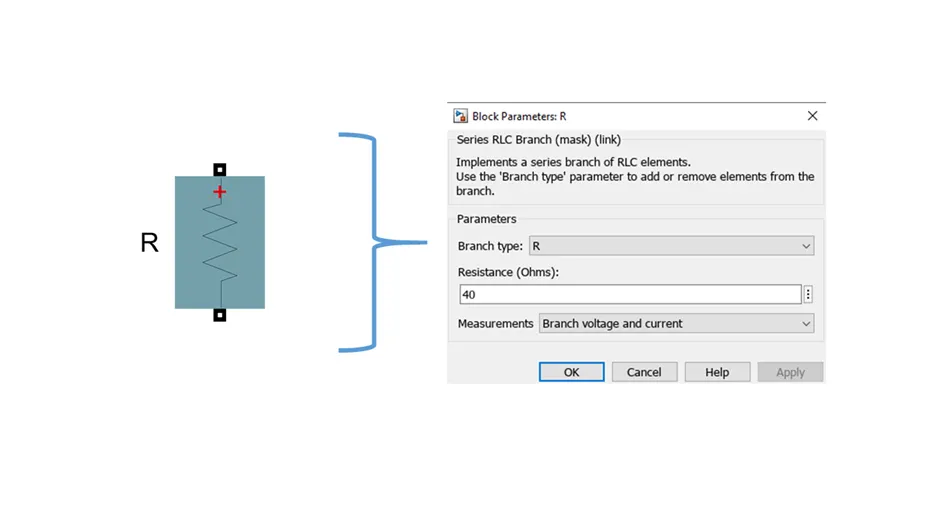
So, the output load Resistance come out to be as,$$ \begin{gathered} R=\frac{V_{\text {out }}^2}{\text { Power }}=\frac{400^2}{4000}=40 \Omega \\ I_{\text {out }}=\frac{\text { Power }}{V_{\text {out }}}=\frac{4000}{400}=10 \mathrm{~A} \end{gathered} $$ Where, Iout=Average output Current Designing of Buck converter in CCM: Duty Ratio: We know that, We know that voltage converter ratio for a Non-Isolated Boost Converter, $$ \frac{V_{\text {out }}}{V_{\text {in }}}=\frac{I_{\text {in }}}{I_{\text {out }}}=\frac{1}{1-D} $$ For Vin = 200V, $$ \begin{gathered} \frac{V_{\text {out }}}{V_{\text {in }}}=\frac{1}{1-D}=\frac{400}{200} \\ D_{\max }=0.5 \end{gathered} $$ For Vin = 300V, $$ \begin{gathered} \frac{V_{\text {out }}}{V_{\text {in }}}=\frac{1}{1-D}=\frac{400}{300} \\ D_{\min }=0.25 \end{gathered} $$ So, the duty ratio range of Boost converter, $$ 0.25 \leq D \leq 0.5 $$ Designing Of Inductor: In Continuous Conduction Mode(CCM), For Inductor current to be continuous, in worst case scenario, $$ I_{\text {Lmin }} \geq \mathbf{0} $$ From waveform we see that, $$ \begin{gathered} I_{L m i n}=I_L-\frac{\Delta i_L}{2} \\ I_L-\frac{\Delta i_L}{2} \geq 0 \end{gathered} $$
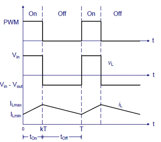
Figure 4- Waveforms of Boost converter
From waveform we see that, $$ \begin{gathered} I_{L m i n}=I_L-\frac{\Delta i_L}{2} \\ I_L-\frac{\Delta i_L}{2} \geq 0 \end{gathered} $$From this, we get the minimum value of inductor such that inductor current will be continuous, $$ L_{m i n} \geq \frac{D(1-D)^2 R}{2 f_s} $$ In the worst-case scenario, the input voltage should be minimum, therefore, the inductor value can be calculated as follows: For D= 0.25, $$ \begin{gathered} L_{\text {min }}=\frac{0.25(1-0.25)^2 \times 40}{2 \times 50 \times 10^3} \\ L_{\text {min }} \approx 56.25 \mu H \end{gathered} $$ For D= 0.5, $$ \begin{gathered} L_{\min }=\frac{0.5(1-0.5)^2 \times 40}{2 \times 50 \times 10^3} \\ L_{\min } \approx 50 \mu H \end{gathered} $$ So, in worst case scenario, we choose the higher value of inductor that is: $$ L_{\text {worst case }} \approx 56.25 \mu \mathrm{H} $$ Assume 40% ripple, then Inductor is, Maximum possible average current in inductor, We observe that in case of Boost Converter, Iin=IL $$ \begin{gathered} \frac{I_L}{I_{\text {out }}}=\frac{1}{1-D_{\max }}=\frac{1}{1-0.5} \\ I_L=20 \mathrm{~A} \\ \Delta i_L=0.4 \times 20 \mathrm{~A} \\ \Delta i_L=8 \mathrm{~A} \end{gathered} $$ To design an Inductor for a specific % of current ripple we use this formula; $$ \begin{gathered} L=\frac{V_{\text {out }}\left(1-D_{\text {max }}\right) D_{\text {max }}}{f_s \cdot \Delta i_L}=\frac{400(1-0.5) 0.5}{50000 \times 8} \\ L=250 \mu H \end{gathered} $$ Where, ∆iL=Ripple current in Inductor
<!--[endif]--><!--[endif]-->
<!--[endif]--><!--[endif]-->
Selection of Inductor:
For selection of an Inductor we are using a quite popular website named “Digikey” one can choose Coilcraft, Mouser and Magnetics as well.
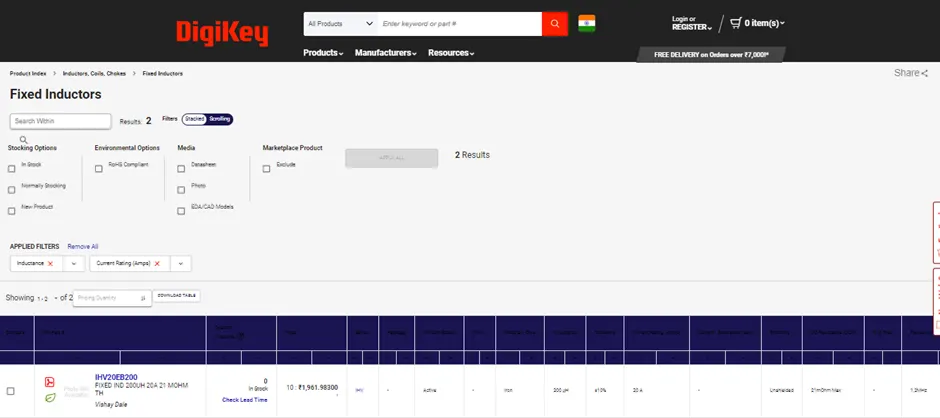
Figure <!-- [if supportFields]> SEQ Figure \* ARABIC <![endif]-->5<!-- [if supportFields]><![endif]-->- Digikey website for selection of Inductor
Go to site and fill the details of this topology and it gives you a suitable list of Inductors based on the ripple % and switching frequency, you can play with the filters to get your desire inductor.
We clearly see that ‘Digikey’ suggesting inductor of 200uH. So we chose this inductor.
We choose Power Inductors– IHV-20-200.
Selected Inductor is L=200μH, for this topology.
Designing of output Capacitor:
Assume that we want output voltage ripple is less than 10%;
We know the output Capacitor formula, $$ C=\left(\frac{D}{R f_s \cdot\left(\frac{\Delta V_{\text {out }}}{V_{\text {out }}}\right)}\right) $$ Where, ∆Vout=Voltage ripple in Capacitor Now, For D= 0.25, $$ \begin{gathered} C_{\text {out }}=\left(\frac{0.25}{40 \times 50 \times 10^3 \cdot(0.1)}\right) \\ C_{\text {out_min }}=1.25 \mu F \end{gathered} $$ For D= 0.5, $$ \begin{gathered} C_{\text {out }}=\left(\frac{0.5}{40 \times 50 \times 10^3 \cdot(0.1)}\right) \\ C_{\text {out_max }} \cong 2.5 \mu F \end{gathered} $$ So we choose maximum value of capacitor that is 2.5μF, but for the safety reason we choose 20% higher than of it; Final choice of output capacitor is, $$ C_{\text {out }}=1.2 \times 2.5 \mu F \approx 3 \mu F $$
Selection of Capacitor:
For Capacitor selection we using website name “Digikey”. It’s quite popular worldwide.
It has a simple GUI with lots of filter to choose a suitable electronic components according to the specification.
We here looking for the ≥3μF capacitor with less ESR(Equivalent series Resistance) and ESL(Equivalent series Inductance).

Figure <!-- [if supportFields]> SEQ Figure \* ARABIC <![endif]-->6<!-- [if supportFields]><![endif]-->- Digikey website for selection of Capacitor
We get the ceramic based surface mount capacitance of value 3μF and withstand voltage capacity of 500V, which is definitely a right choice for this topology.
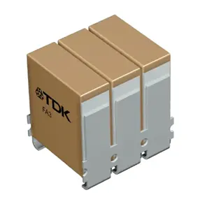
Figure <!-- [if supportFields]> SEQ Figure \* ARABIC <![endif]-->7<!-- [if supportFields]><![endif]-->- 3μF ±20@0V Fast Switching Capacitor-Flex Assembly (FA) series
Selected Capacitor is C=3μF, for this topology.
Designing of MOSFET:
First we focus on the suitable selection of MOSFET, one can chose IGBT as well.
We required,
Blocking Voltage:
According to given topology specs, during turn “OFF”, the MOSFET maximum blocking voltage comes out to be 400V, but for the safety reason we choose the MOSFET whose value is 50% higher than the maximum blocking voltage, so we have;
$$ V_{\text {Blocking }}=1.5 \times 400=600 \mathrm{~V} $$ From this we observe that the drain to source voltage of MOSFET should be as, $$ V_{D S} \geq 600 V $$ Peak current in MOSFET: According to the circuit of the Boost Converter, we can easily find the MOSFET peak current that could flow during "ON" condition. In this case we observe that the peak current of converter inductor should be same as the peak current of the MOSFET, that is; So we know that the maximum Inductor current formula as; $$ I_{L_{-} \max }=I_L+\frac{\Delta i_L}{2}=I_{\text {mosfet_peak }} $$ Where, $$ \begin{aligned} & I_{\text {mosfet_peak }}=\text { Peak MOSFET Current } \\ & \qquad \begin{array}{r} I_{\text {mosfet_peak }}=\mathbf{2 0}+\frac{\mathbf{8}}{\mathbf{2}} \\ I_{\text {mosfet_peak }}=\mathbf{2 4 A} \end{array} \end{aligned} $$
<!--[endif]--><!--[endif]-->
Selection of MOSFET:
After getting some essential data for the MOSFET, we looking for the searching of MOSFET and we choose the website “Infineon”, one can choose “Mouser” or “Digikey” as well,
Suitable MOSFET that we chose as
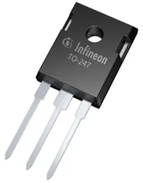
Figure <!-- [if supportFields]> SEQ Figure \* ARABIC <![endif]-->8<!-- [if supportFields]><![endif]-->- High voltage CoolMOS™ superjunction MOSFET, 600V
Features of MOSFET IPW60R037CSFD:
<!-- [if !supportLists]-->· <!--[endif]-->Ultra-fast body diode
<!-- [if !supportLists]-->· <!--[endif]-->Best-in-class reverse recovery charge (Qrr)
<!-- [if !supportLists]-->· <!--[endif]-->Low parasitic inductance.
From datasheet of IPW60R037CSFD MOSFET, some the following parameters are observed;
Table <!-- [if supportFields]> SEQ Table \* ARABIC <![endif]-->1<!-- [if supportFields]><![endif]-->- Key Performance Parameters
|
Parameter |
Symbol |
Values |
Unit |
|
Drain to source voltage |
VDS |
600 |
V |
|
Continuous drain current |
ID |
25 |
A |
|
Drain to source resistance |
RDS(on) |
31 |
mΩ |
|
Gate to source voltage |
VGS |
15 |
V |
|
Gate resistance |
RG |
3.9 |
Ω |
|
Input capacitance |
Ciss |
5623 |
pF |
|
Output capacitance |
Coss |
104 |
pF |
|
Power dissipation |
Ptot |
245 @ 25oC |
W |
|
Turn on delay time |
td(on) |
53 |
ns |
|
Turn off delay time |
td(off) |
196 |
ns |
|
Rise time |
tr |
30 |
ns |
|
Fall time |
tf |
6 |
ns |
|
Reverse Recovery time |
trr |
168 |
ns |
From the above table VGS, RG, Ciss, Coss and Crss and some other parameters are help to find the suitable Gate Driver for this topology.
Selection of Output Diode:
To reduce losses, Schottky diodes should be used. The forward current rating needed is equal to the maximum output current:
IF = IOUT(max)
Where,
IF = average forward current of the rectifier diode
IOUT(max) = maximum output current necessary in the application
Schottky diodes have a much higher peak current rating than average rating. Therefore the higher peak current in the system is not a problem.
Table <!-- [if supportFields]> SEQ Table \* ARABIC <![endif]-->2<!-- [if supportFields]><![endif]-->- Parameters from the datasheet of Diode
|
Parameter |
Symbol |
FR30G(R)02 |
Unit |
|
Repetitive peak reverse voltage |
VRRM |
400 |
V |
|
RMS reverse voltage |
VRMS |
280 |
V |
|
DC blocking voltage |
VDC |
400 |
V |
|
Continuous forward current |
IF |
30 |
A |
|
Diode forward voltage |
VF |
1 |
V |
|
Reverse recovery time |
trr |
200 |
ns |
Designing of Gate Driver:
Gate driver designing is totally based on the selection of MOSFET, we already select the MOSFET ‘BSF450NE7NH3 G’. Before choosing the Gate driver first we see some interesting features of an ideal Gate Driver:
Ideal Gate Driver features:
<!-- [if !supportLists]-->1. <!--[endif]-->It should have a capability of Level shifting.
<!-- [if !supportLists]-->2. <!--[endif]-->Meet the voltage and current requirements of the gate emitter/source region.
<!-- [if !supportLists]-->3. <!--[endif]-->It should have a capability to deal with floating supply.
<!-- [if !supportLists]-->4. <!--[endif]-->High Input Impedance.
<!-- [if !supportLists]-->5. <!--[endif]-->High CMTI(Common-Mode Transient Immunity).
Gate drivers are broadly classified in two types:
<!-- [if !supportLists]-->1. <!--[endif]-->Non- Isolated Gate Driver.
<!-- [if !supportLists]-->2. <!--[endif]-->Isolated Gate Driver
We always prefer an isolated gate driver over non-isolated gate driver if there is no economic constrain. Because isolated gate driver has a capability to isolate the converter from the microcontroller and it has a long life cycle as compare to non-isolated gate driver.
Selection of Gate Driver:
Gate driver choice is depends on the parameters of MOSFET like Input capacitance, output capacitance, reverse transfer capacitance , gate to source threshold voltage, gate resistance, delay time, rise time and net charge etc. These parameters are already given in the datasheet of the MOSFET as discussed above.
For making Boost converter or step-up converter we select single-channel high-speed low-side Gate Driver that is UCC27511A.
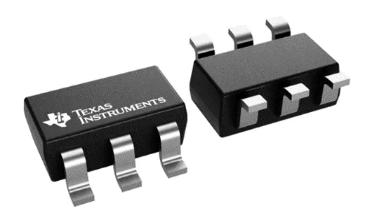
Figure <!-- [if supportFields]> SEQ Figure \* ARABIC <![endif]-->9<!-- [if supportFields]><![endif]-->- Gate Driver UCC27511A
Reasons for choosing Gate Driver UCC27511A:
From the datasheet of this gate driver we analyse the following below points;
<!-- [if !supportLists]-->1. <!--[endif]-->According to given topology, we required a power supply to activate this IC and we choose 15V power supply, one can use the Bootstrap method to given the power supply from the existing power supply.
<!-- [if !supportLists]-->2. <!--[endif]-->Other parameters are given in the datasheet of this driver;
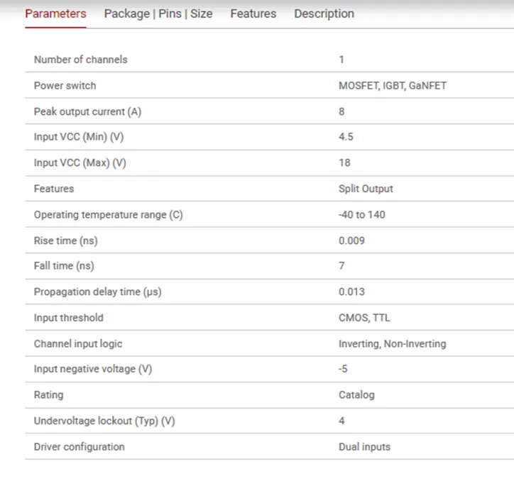
Figure <!-- [if supportFields]> SEQ Figure \* ARABIC <![endif]-->10<!-- [if supportFields]><![endif]-->- Gate Driver parameters
<!-- [if !supportLists]-->3. <!--[endif]-->UCC27511A device is an automotive-grade single-channel low-side, high-speed gate driver rated for MOSFETs, IGBTs, and emerging wide-bandgap power devices such as GaN.
<!-- [if !supportLists]-->4. <!--[endif]-->The device features fast Glitch-Free Operation at Power Up and Power rise times, fall times, and propagation delays, making device suitable for high-speed applications.
<!-- [if !supportLists]-->5. <!--[endif]-->The split output configuration enables easy and independent adjustment of rise and fall times using only two resistors and eliminating the need for an external diode.
Pin Configuration:
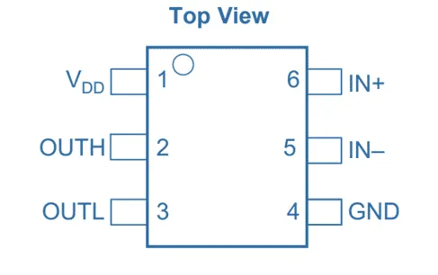
Figure 10- PIN diagram of UCC27511A
Pin Function:
<!-- [if !supportLists]-->1. <!--[endif]-->VDD: This is the power supply voltage input pin for the device. The voltage range for VDD is between 4.5V and 18V.
<!-- [if !supportLists]-->2. <!--[endif]-->IN+: Non-Inverting Input
<!-- [if !supportLists]-->3. <!--[endif]-->IN-: Inverting Input
<!-- [if !supportLists]-->4. <!--[endif]-->OUTH: Sourcing current output of driver. Connect a resistor between the OUTH pin and the gate of the power switching device to adjust turn on speed.
<!-- [if !supportLists]-->5. <!--[endif]-->OUTL: Sinking current output of driver. Connect a resistor between the OUTL pin and the gate of the power switching device to adjust turn off speed.
<!-- [if !supportLists]-->6. <!--[endif]-->GND: Ground.
Typical Application Diagrams:
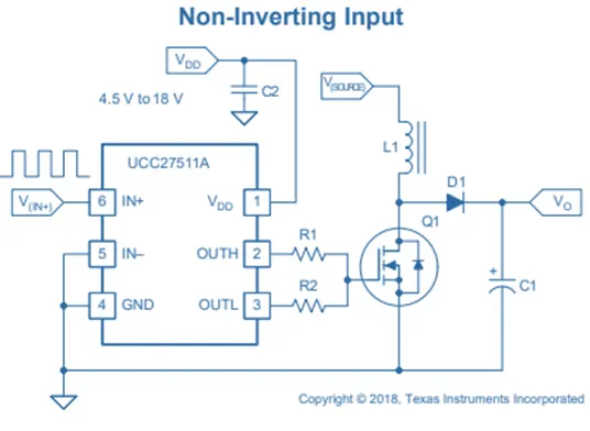
Figure <!-- [if supportFields]> SEQ Figure \* ARABIC <![endif]-->12<!-- [if supportFields]><![endif]-->- Gate driver schematic for non-inverting Input
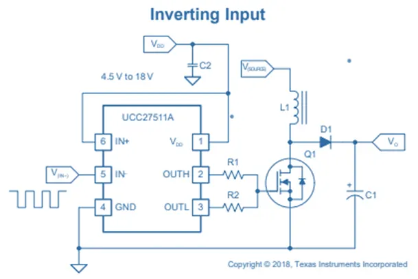
Figure <!-- [if supportFields]> SEQ Figure \* ARABIC <![endif]-->13<!-- [if supportFields]><![endif]-->- Gate driver schematic for inverting Input
Controller Design:
In order to get the stability of a Boost converter or any type of system, it’s always good to do transient and steady-state analysis, this will tell you the overall behaviour of a system. Although there are various type of close loop techniques available in the real world, but the basic structure is common in all of the close loop technique that is;
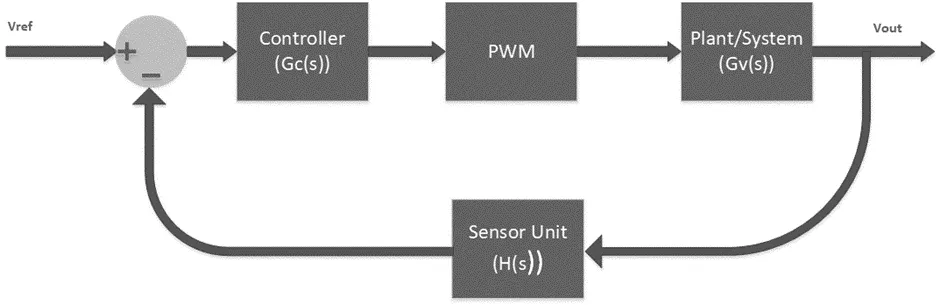
Figure <!-- [if supportFields]> SEQ Figure \* ARABIC <![endif]-->14<!-- [if supportFields]><![endif]-->- Block diagram of Closed-loop System
Procedure:
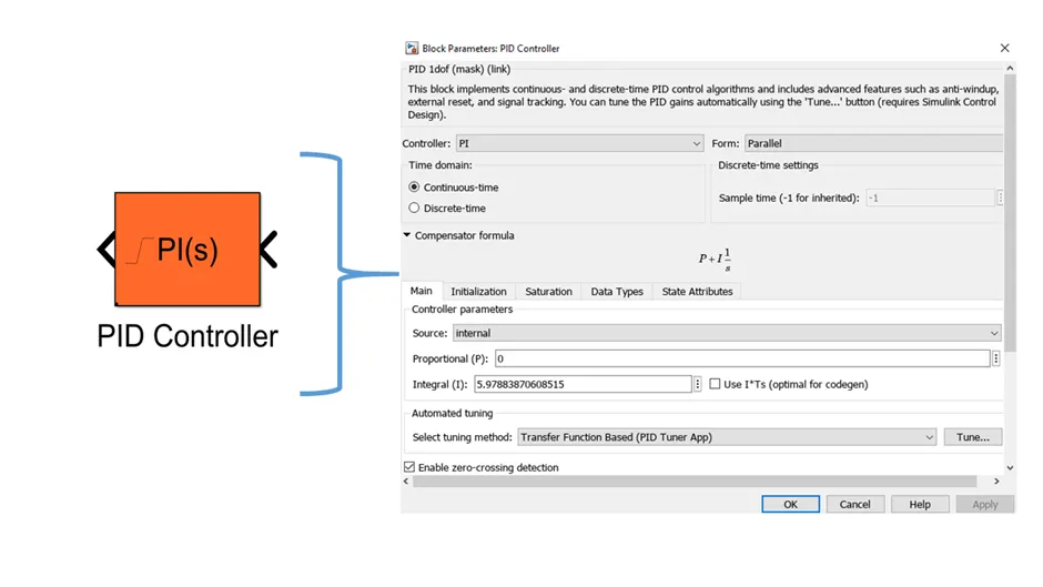
Step-01: Find the Control voltage Transfer function $(\mathrm{Gd}(\mathrm{s}))$ of the Boost Converter; We know from the previous Challenges, the control voltage transfer function is, $$ G_d(s)=\frac{-\frac{I_L}{C}\left(s-\frac{(1-D) V_C}{L \cdot I_L}\right)}{\left(s^2+\frac{s}{R C}+\frac{(1-D)^2}{L C}\right)} $$ Step-02: After finding Transfer function we have to find PI Controller Transfer function as; $$ \begin{gathered} G_c(s)=K_P+\frac{K_I}{s} \\ G_c(s)=\frac{\left(K_P\right) s+K_I}{s} \end{gathered} $$ Step-03: Now, we have to find controller Gain parameters $\left(K_P, K_D\right)$. In order to find that, we here, using MATLAB Autotune option which is belong under the window of PID controller block. Hence we know all the parameters values such as; $$ \begin{gathered} \mathrm{Vc}=\text { Vout }=400 ; \quad \mathrm{IL}=20 \mathrm{~A} ; \quad \mathrm{R}=40 \Omega ; \quad \mathrm{L}=200 \mu \mathrm{H} ; \quad \mathrm{C}=3 \mu \mathrm{F} ; \\ \mathrm{D}=(0.5+0.25) / 2=0.375 \\ G_d(s)=\frac{-\frac{I_L}{C}\left(s-\frac{(1-D) V_C}{L \cdot I_L}\right)}{\left(s^2+\frac{s}{R C}+\frac{(1-D)^2}{L C}\right)} \\ G_d(s)=\frac{-5.333 \times 10^6(s-62500)}{\left(s^2+8333.33 \mathrm{~s}+5.208 \times 10^8\right)} \end{gathered} $$ $$ \begin{gathered} G_d(s)=\frac{-\frac{I_L}{C}\left(s-\frac{(1-D) V_c}{L \cdot I_L}\right)}{\left(s^2+\frac{s}{R C}+\frac{(1-D)^2}{L C}\right)} \\ G_d(s)=\frac{-5.333 \times 10^6(s-62500)}{\left(s^2+8333.33 s+5.208 \times 10^8\right)} \end{gathered} $$
<!--[endif]--><!--[endif]-->
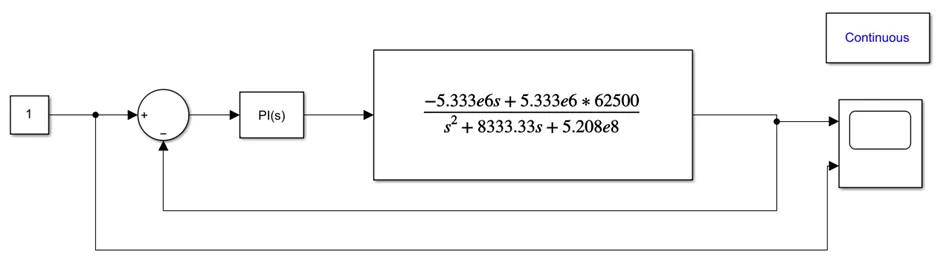
Figure 15- Testing, Response of a signal through step signal
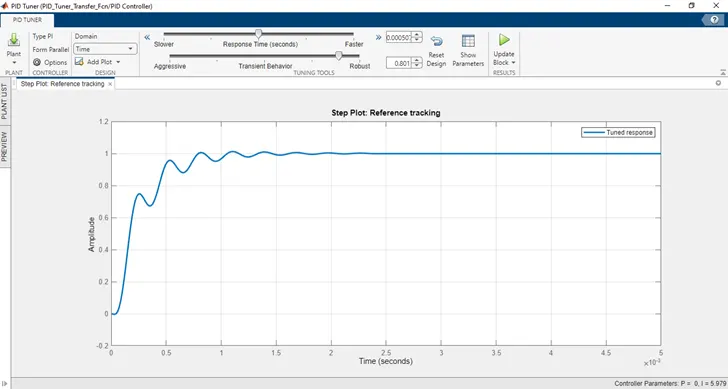
Figure 16- System Response after testing
Step-04: The output of a PID controller given to the PWM DC-DC Generator block which generate required PWM pulses for given duty ratio. And this PWM is given to Gate driver and Gate driver output is produce gate pulses for the Gate terminal of the MOSFET.
Schematic of closed loop Non-Isolated Buck Converter:
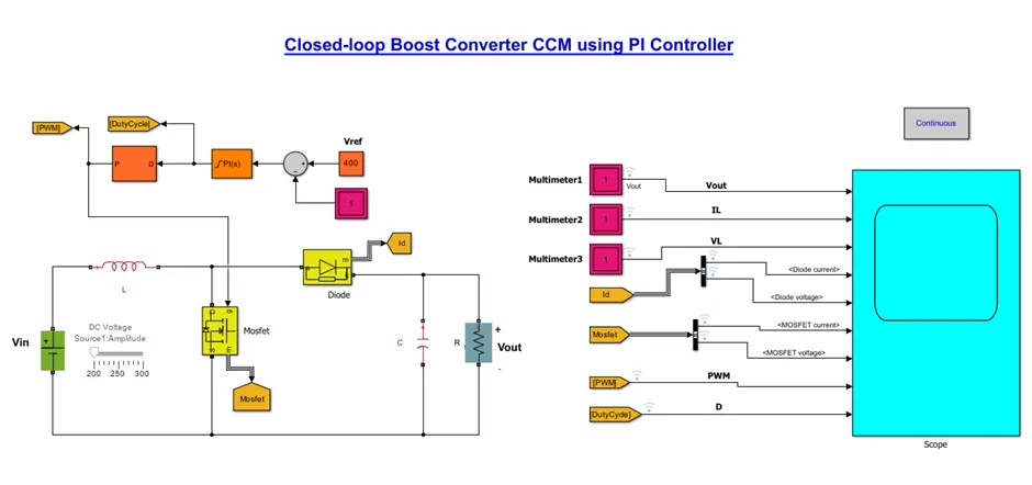
Used Blocks and Parameters value:
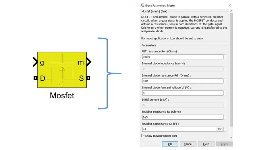
<!-- [if !supportLists]-->· <!--[endif]-->MOSFET:
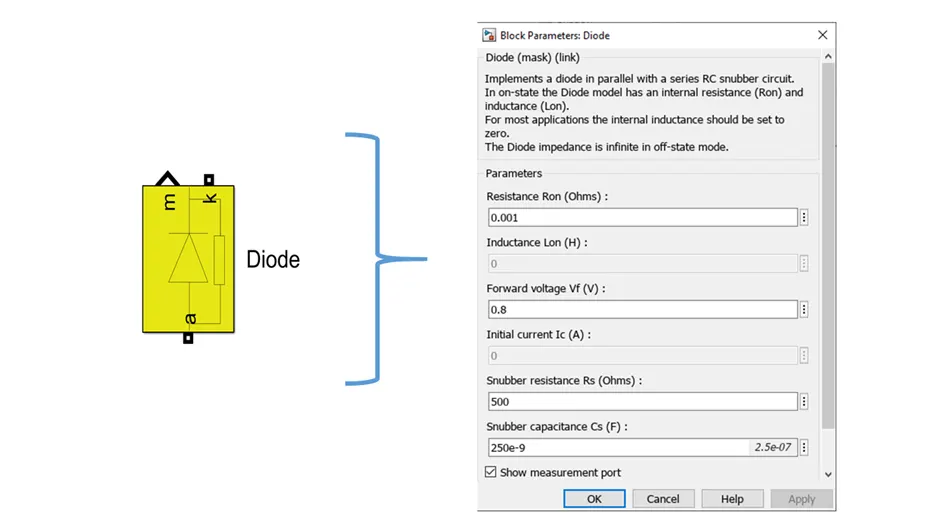
<!-- [if !supportLists]-->· <!--[endif]-->Diode:
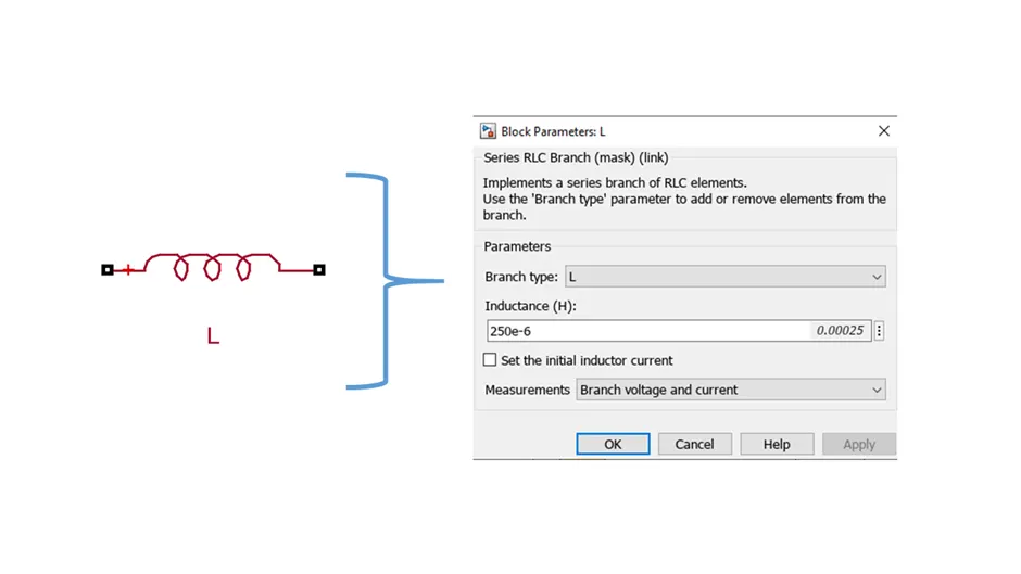
<!-- [if !supportLists]-->· <!--[endif]-->Inductor:
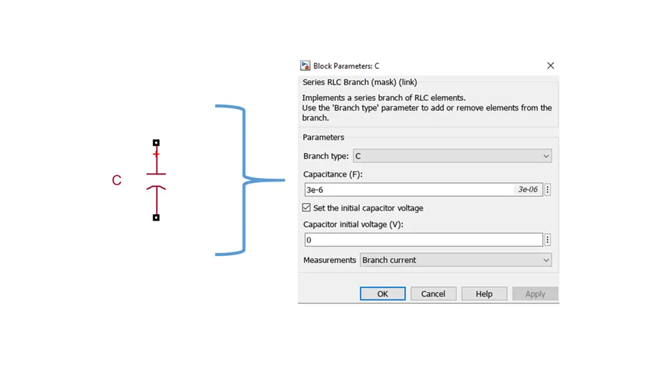
<!-- [if !supportLists]-->· <!--[endif]-->Capacitor:
<!-- [if !supportLists]-->· <!--[endif]-->Load Resistance:
<!-- [if !supportLists]-->· <!--[endif]-->PID Controller:
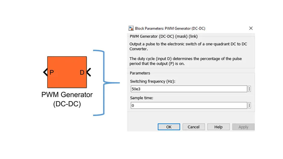
<!-- [if !supportLists]-->· <!--[endif]-->PWM Generator (DC-DC):
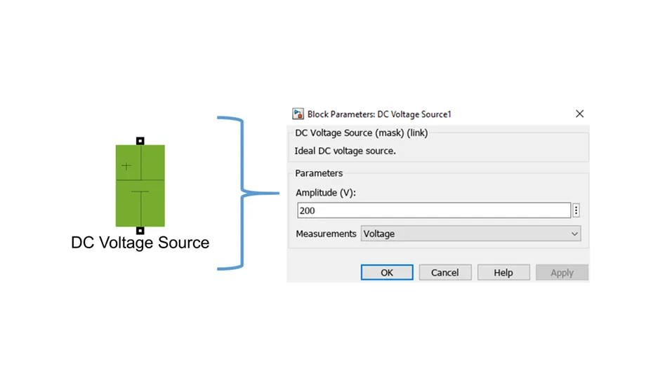
<!-- [if !supportLists]-->· <!--[endif]-->Input Voltage:
Result:
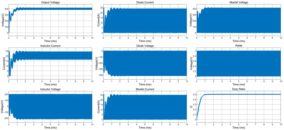
We run this Simulation for 10ms and we got the desire result as following:
Case-01:
For Vin = 200V,
Zoom-OUT:
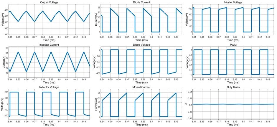
Zoom-IN:
Output Voltage and Output Current:
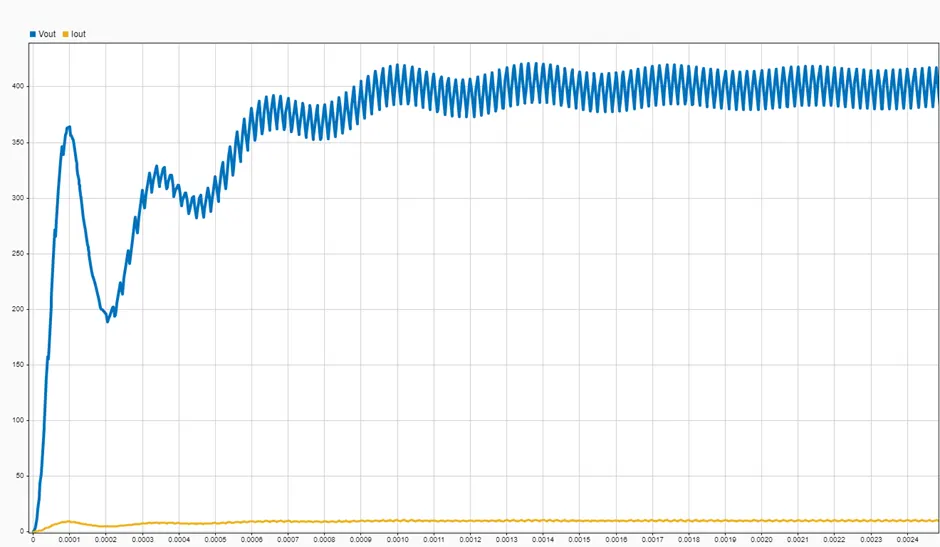
<!-- [if !supportLists]-->· <!--[endif]-->In this topology, we clearly see that the output voltage waveform during transient have not any peak overshoot. It catches the steady state smoothly.
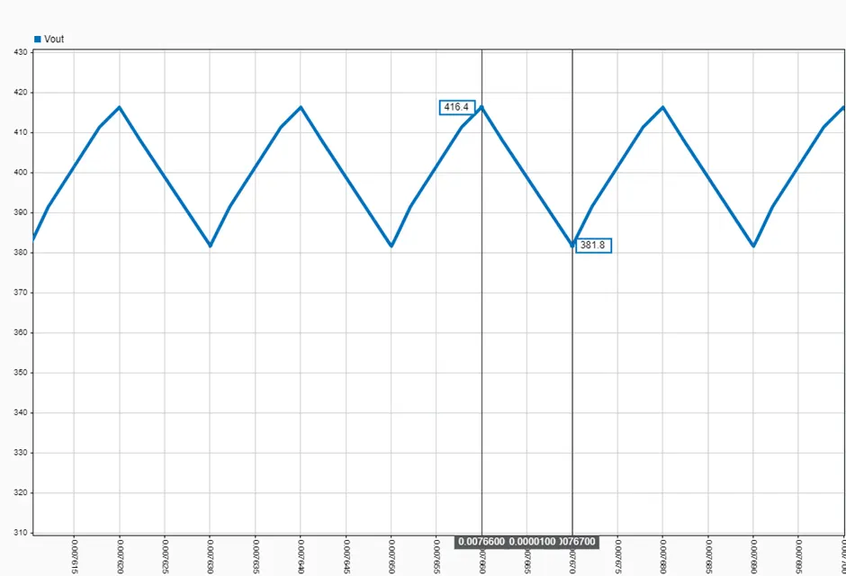
<!-- [if !supportLists]-->· <!--[endif]-->In steady state, the output voltage is approximately 400V, and ripples are also less than 10%.
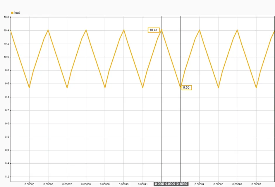
<!-- [if !supportLists]-->· <!--[endif]-->Since the load here is resistive therefore, the output current waveform nature is same as the output voltage waveform and the observed average output current is around 10A, which is similar as we calculated above in theory part.
Inductor Voltage and Inductor Current:
<!-- [if !supportLists]-->· <!--[endif]-->At steady state, the average inductor current is approximately equal to the average input current that is 20A.
$$ \begin{gathered} I_{L \max }=24.40 \mathrm{~A} \\ I_{L \min }=16.40 \mathrm{~A} \\ \Delta i_L=8 \mathrm{~A} \end{gathered} $$
<!-- [if !supportLists]-->· <!--[endif]-->Inductor ripple current is approximate 39% which is less than the 40% of the ripple.
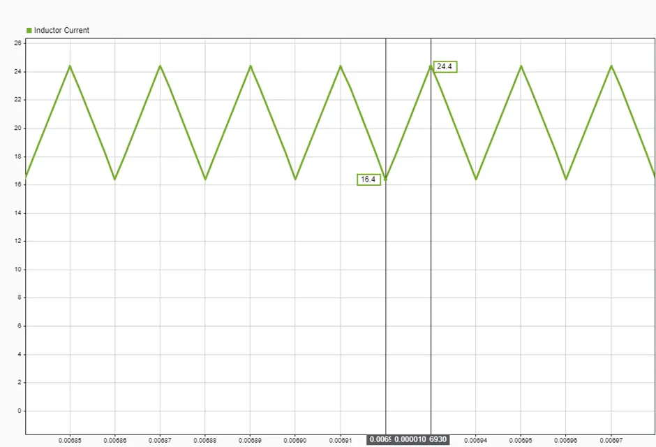
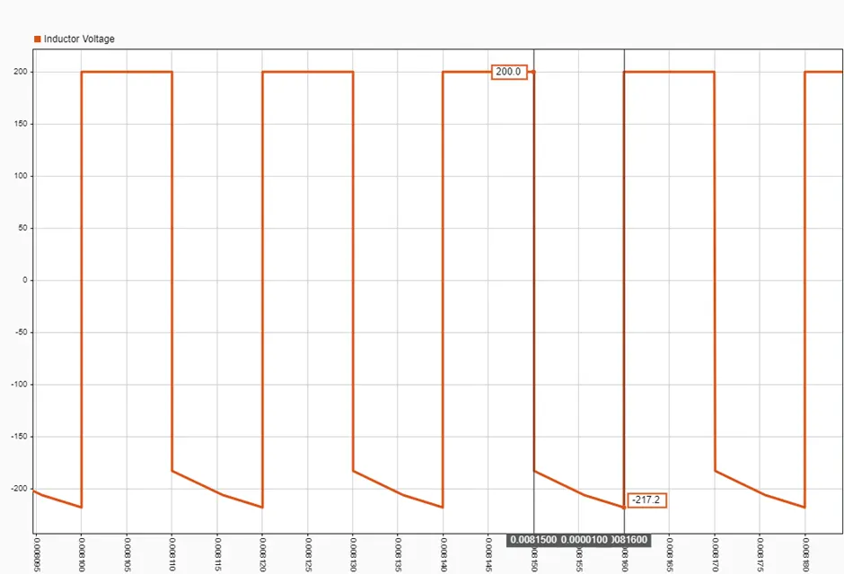
<!-- [if !supportLists]-->· <!--[endif]-->In the below plot we seen that the inductor voltage is 200V when, MOSFET is “ON” and Diode is “OFF” and when MOSFET is “OFF” and Diode is “ON”, inductor voltage is -217.2V. But in theoretically during turn ON voltage came 200V and turn OFF voltage came out to -200V.
MOSFET Voltage and MOSFET Current:
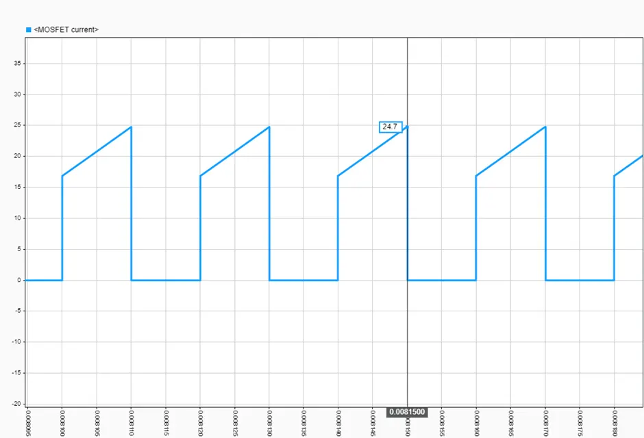
<!-- [if !supportLists]-->· <!--[endif]-->In theoretically, MOSFET peak current came out to 24A, but due to presence of non-ideality in this converter we see that in above plot the peak MOSFET current is around 24.7A.
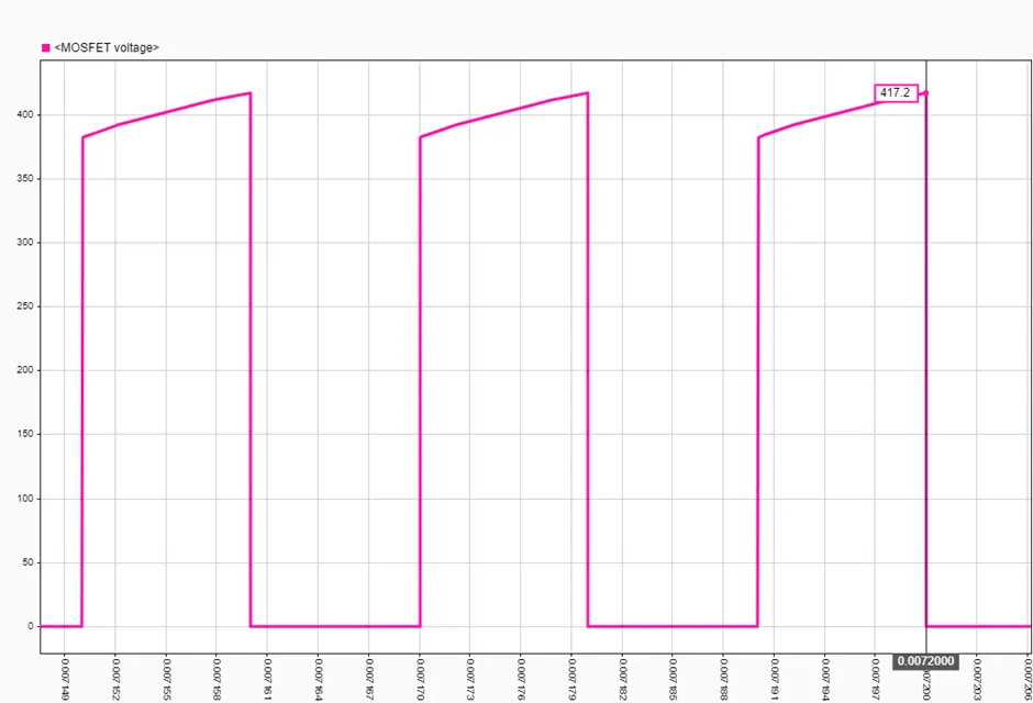
<!-- [if !supportLists]-->· <!--[endif]-->In the above plot of MOSFET voltage, we clearly see that the peak MOSFET voltage is 417.2V and in theory voltage came out to 400V.
<!-- [if !supportLists]-->· <!--[endif]-->So we observe that our choosen MOSFET and their ratings are appropriate for this topology.
Diode Voltage and Diode Current:
<!-- [if !supportLists]-->· <!--[endif]-->In the below plot we observe that the Diode and MOSFET wave shape are similar in nature except MOSFET operates, during Turn ON and Diode Operates during Turn OFF.
<!-- [if !supportLists]-->· <!--[endif]-->Diode peak current is same as MOSFET peak Current which is around 23.9A.
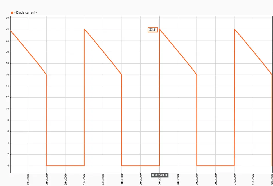
<!-- [if !supportLists]-->· <!--[endif]-->In the below plot of Diode voltage is similar to plot of MOSFET voltage with same magnitude but opposite in nature.
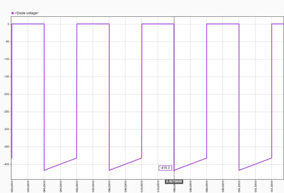
<!-- [if !supportLists]-->· <!--[endif]-->Diode peak inverse voltage is around 416.3V.
Capacitor Current and Capacitor Voltage:
<!-- [if !supportLists]-->· <!--[endif]-->In the below plot of capacitor current we observe that the peak current is less than 15A and wave shape is trapezoidal in nature that shows the charging and discharging of charge during each cycle.
$$ \begin{gathered} I_{C \max }=14.9 A \\ I_{C \min }=-10.9 A \\ \Delta i_C=25.8 A \end{gathered} $$
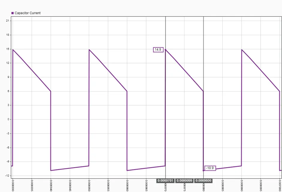
<!-- [if !supportLists]-->· <!--[endif]-->Capacitor voltage plot is similar to the plot of output voltage as discussed above because load resistance and capacitor are connected parallel to each other.
PWM and Duty Ratio:
<!-- [if !supportLists]-->· <!--[endif]-->PWM is generated by PWM Generator(DC-DC) block where input of this block is controlled duty cycle, produced by the PI controller block.
<!-- [if !supportLists]-->· <!--[endif]-->In the below plot we see that PWM is generated with a switching frequency of 50KHz in the range of (0-1)V.
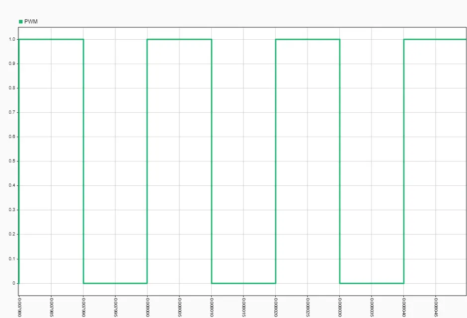
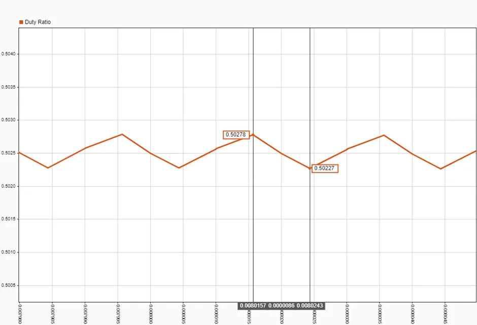
<!-- [if !supportLists]-->· <!--[endif]-->In the below plot of Duty Ratio(D), we observe that for the input voltage of 200V the average duty ratio is approximately equal to 0.5025, which is approximately same as when we find duty ratio theoretically.
Case-02:
For Vin = 300V,
Zoom-OUT:
Zoom-IN:
Output Voltage and Output Current:
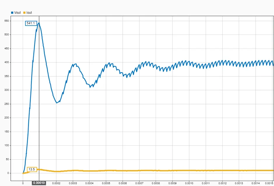
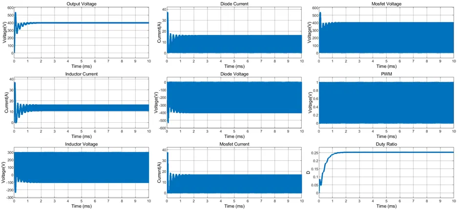
<!-- [if !supportLists]-->· <!--[endif]-->In this case, we clearly see that the output voltage waveform during transient have maximum peak overshoot of voltage 541.1V. After some oscilation output voltage waveform approaches steady state voltage that is 400V.
<!-- [if !supportLists]-->· <!--[endif]-->In the above plot we also see that during transient the output current peak value is approximately 13.5A
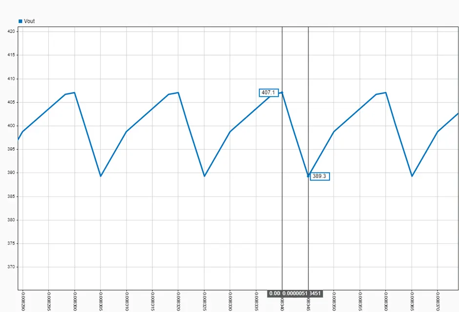
<!-- [if !supportLists]-->· <!--[endif]-->In steady state, the output voltage is approximately 398.2V, and ripples are also less than 10%.
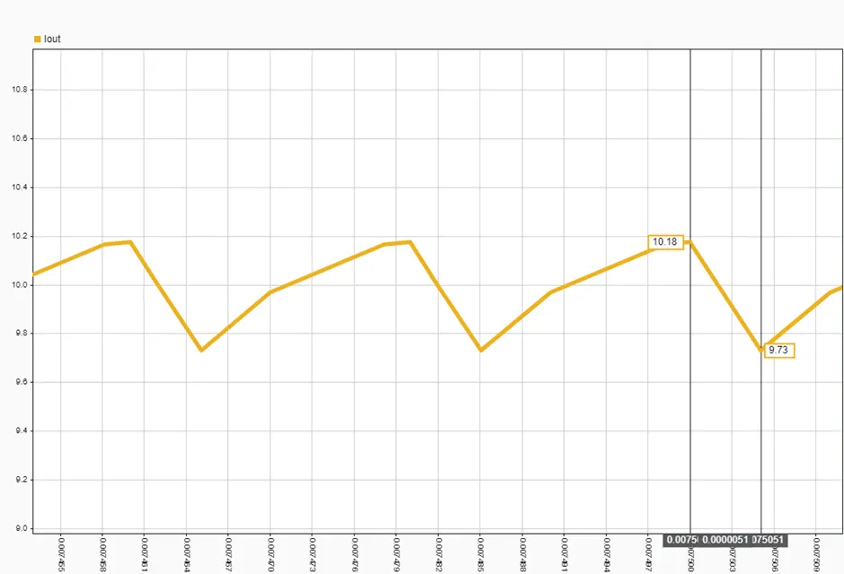
<!-- [if !supportLists]-->· <!--[endif]-->Since the load here is resistive therefore, the output current waveform nature is same as the output voltage waveform and the observed average output current is around 9.95A, which is similar as we calculated above in theory part.
Inductor Voltage and Inductor Current:
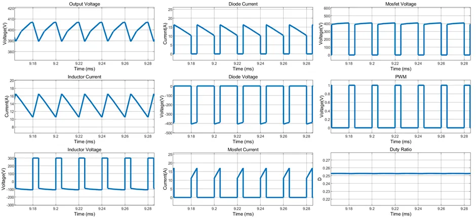
<!-- [if !supportLists]-->· <!--[endif]-->At steady state, the average inductor current is approximately equal to the average input current that is 20A.
$$ \begin{aligned} & I_{L \max }=16.50 \mathrm{~A} \\ & I_{L \min }=10.50 \mathrm{~A} \\ & \Delta i_L=6 A \end{aligned} $$
<!-- [if !supportLists]-->· <!--[endif]-->Inductor ripple current is approximate 44% which is due to non-idealities of the switches.
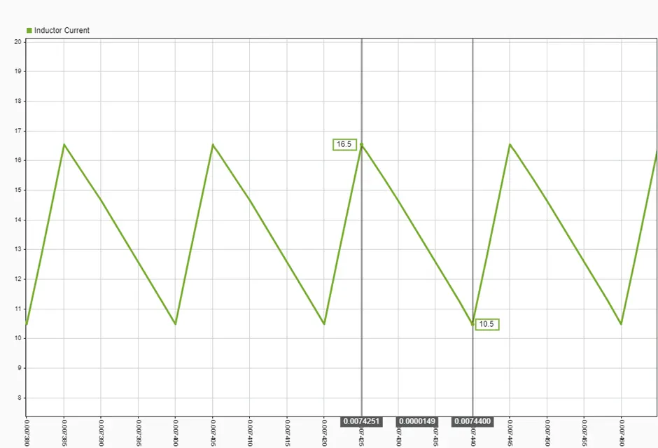
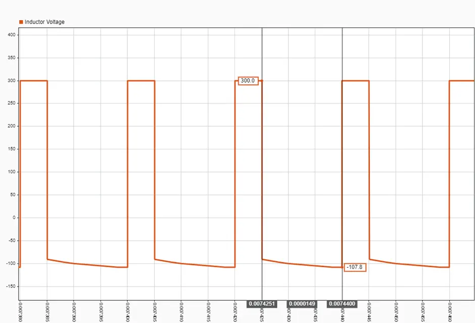
<!-- [if !supportLists]-->· <!--[endif]-->In the below plot we seen that the inductor voltage is 300V when, MOSFET is “ON” and Diode is “OFF” and when MOSFET is “OFF” and Diode is “ON”, inductor voltage is -107.8V. But in theoretically during turn ON voltage came 300V and turn OFF voltage came out to -100V.
MOSFET Voltage and MOSFET Current:
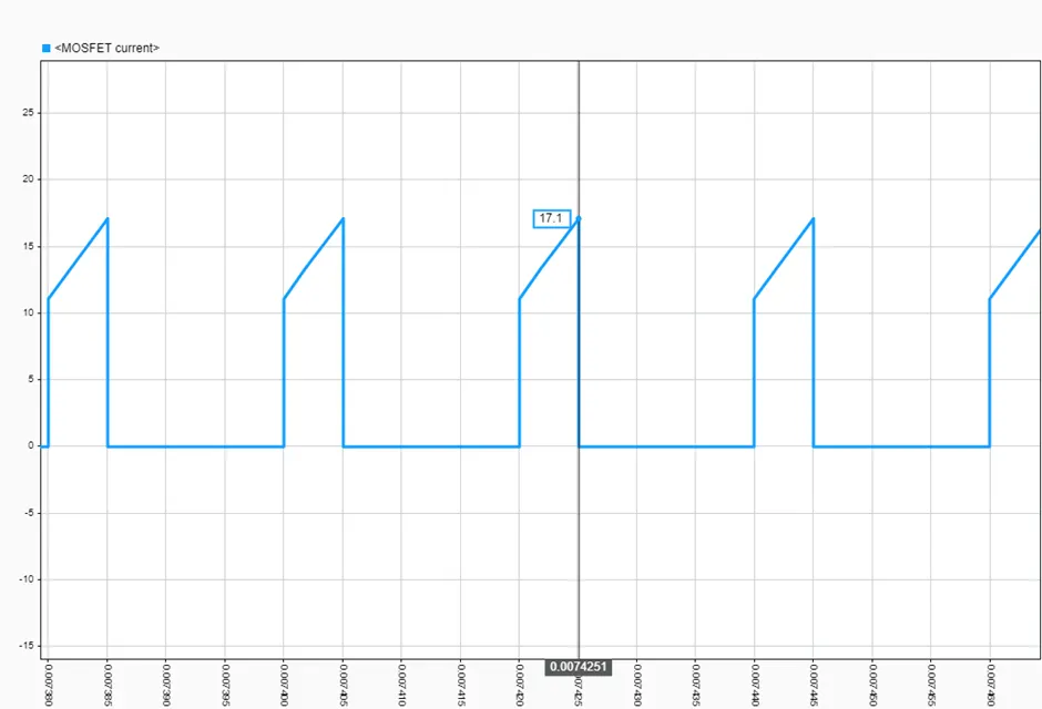
<!-- [if !supportLists]-->· <!--[endif]-->In theoretically, MOSFET peak current is equivalent to inductor peak current but due to presence of non-ideality in this converter we see that in above plot the peak MOSFET current is around 17.1A but in case of inductor peak current, it comes around 16.5V
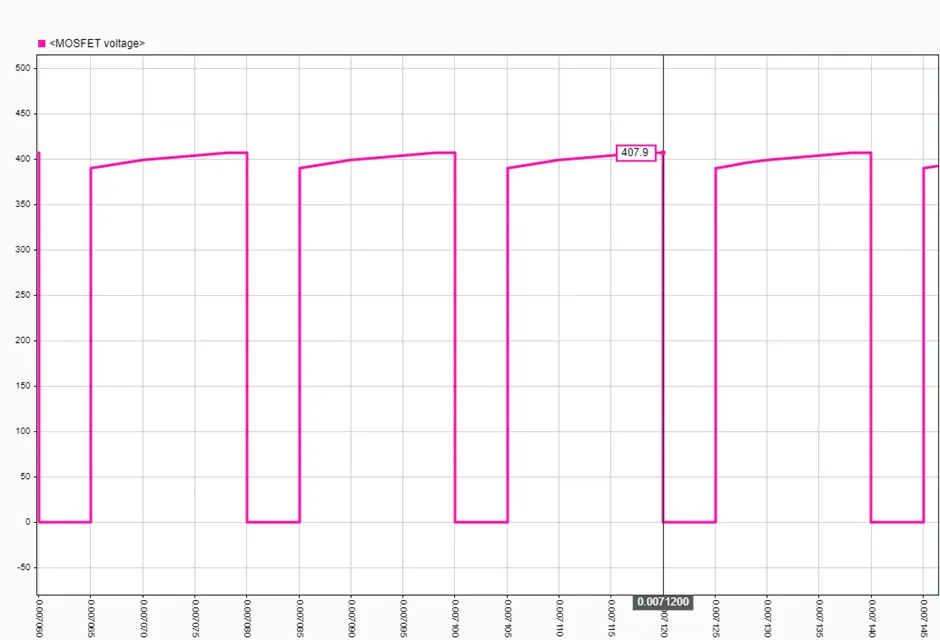
<!-- [if !supportLists]-->· <!--[endif]-->In the above plot of MOSFET voltage, we clearly see that the peak MOSFET voltage is 407.9V and in theory voltage came out to 400V.
<!-- [if !supportLists]-->· <!--[endif]-->So we observe that our chosen MOSFET and their ratings are appropriate for this topology.
Diode Voltage and Diode Current:
<!-- [if !supportLists]-->· <!--[endif]-->In the below plot we observe that the Diode and MOSFET wave shape are similar in nature except MOSFET operates, during Turn ON and Diode Operates during Turn OFF.
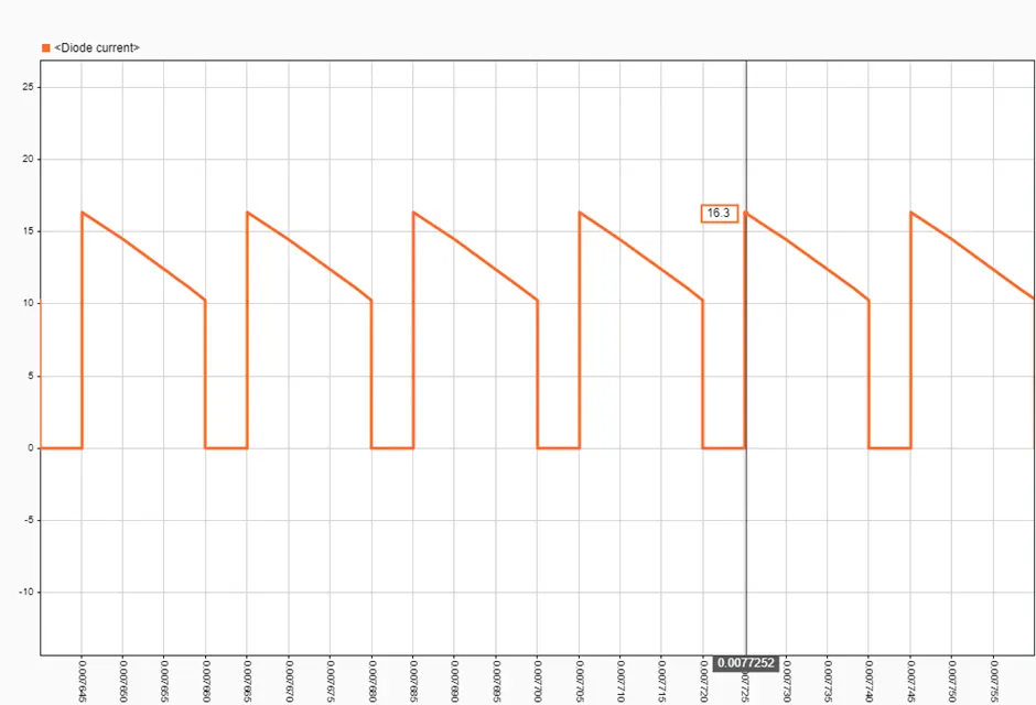
<!-- [if !supportLists]-->· <!--[endif]-->Diode peak current is same as Inductor peak Current which is around 16.3A.
<!-- [if !supportLists]-->· <!--[endif]-->In the below plot of Diode voltage is similar to plot of MOSFET voltage with same magnitude but opposite in nature.
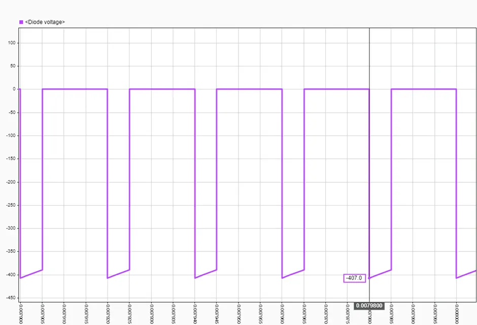
<!-- [if !supportLists]-->· <!--[endif]-->Diode peak inverse voltage is around 407V.
Capacitor Current and Capacitor Voltage:
<!-- [if !supportLists]-->· <!--[endif]-->In the below plot of capacitor current we observe that the peak current is less than 15A and wave shape is trapezoidal in nature that shows the charging and discharging of charge during each cycle.
$$ \begin{aligned} & I_{C \max }=6.8 A \\ & I_{C \min }=-10.8 A \\ & \Delta i_C=17.6 A \end{aligned} $$
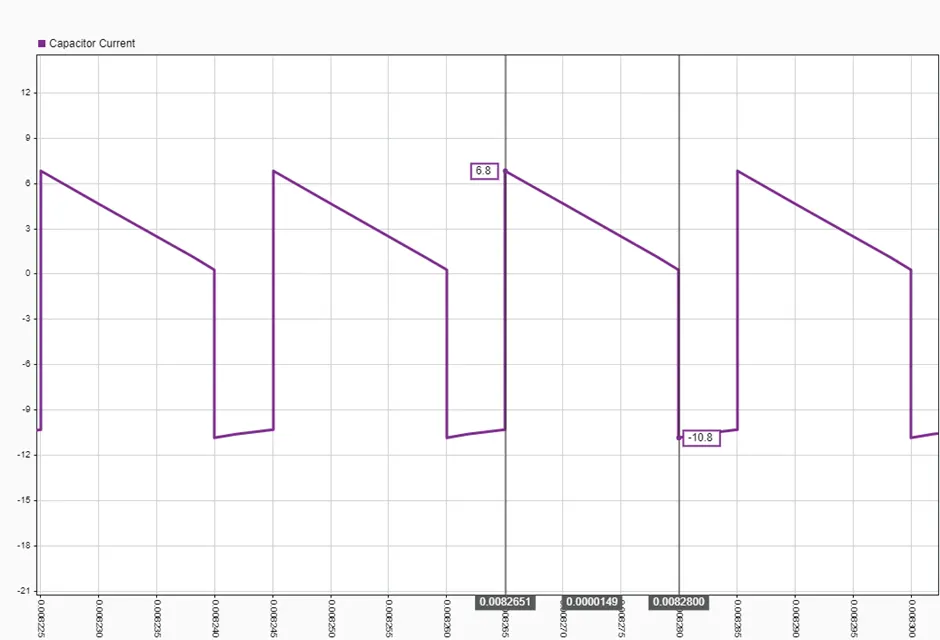
<!-- [if !supportLists]-->· <!--[endif]-->Capacitor voltage plot is similar to the plot of output voltage as discussed above because load resistance and capacitor are connected parallel to each other.
PWM and Duty Ratio:
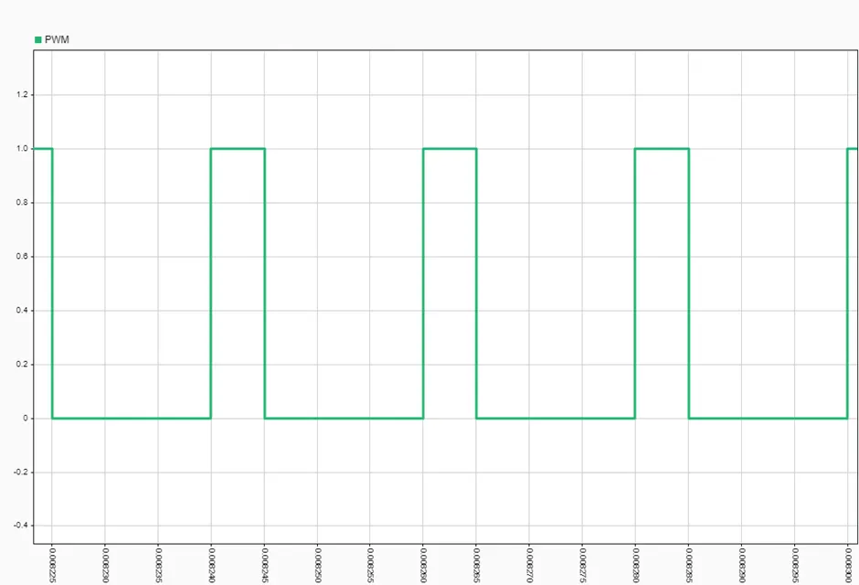
<!-- [if !supportLists]-->· <!--[endif]-->PWM is generated by PWM Generator(DC-DC) block where input of this block is controlled duty cycle, produced by the PI controller block.
<!-- [if !supportLists]-->· <!--[endif]-->In the below plot we see that PWM is generated with a switching frequency of 50KHz in the range of (0-1)V.
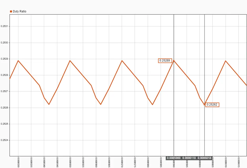
<!-- [if !supportLists]-->· <!--[endif]-->In the below plot of Duty Ratio(D), we observe that for the input voltage of 200V the average duty ratio is approximately equal to 0.2527, which is approximately same as when we find duty ratio theoretically.
Loss Calculation of a Boost Converter:
The following parameters are observed from the above calculations, summarize in following table:
Table <!-- [if supportFields]> SEQ Table \* ARABIC <![endif]-->3<!-- [if supportFields]><![endif]-->- Key parameters of boost converter
|
Parameters |
Symbol |
For, Vin = 200V |
For, Vin = 300V |
|
Duty Ratio |
D |
0.5 |
0.25 |
|
Output Current |
Iout |
10A |
10A |
|
Switch/fet Current |
Isw |
20A |
13.33A |
|
Inductor Ripple Current |
∆iL |
8A |
5.332 |
|
Maximum Switch/fet Current |
Isw(max) |
24A |
16A |
|
Switching Frequency |
fs |
50kHz |
50KHz |
The power losses can be calculated as follows:
Switch loss:
The switch loss consists of the conduction loss and the switching loss. The conduction loss is the product of the drain to source resistance, the duty cycle, and the square of the average switch current. The switching loss is the product of the input voltage, the peak switch current, the switching frequency, and a factor that depends on the turn on and turn off times of the switch. The switch loss can be expressed as:$$ P_{S W}=R_{D S(\text { on })} D I_{S W}^2+V_{I N} I_{S W(\text { peak })} f_S\left(\frac{t_{d(\text { on })}+t_r}{2}+\frac{t_{d(\text { off })}+t_f}{2}\right) $$Where,$$ \begin{aligned} & P_{S W}=\text { switch loss } \\ & R_{D S(o n)}=\text { drain to source resistance } \\ & D=\text { duty cycle } \\ & I_{S W}=\text { average switch current } \\ & V_{I N}=\text { input voltage } \\ & I_{S W \text { (peak) }}=\text { peak switch current } \\ & f_S=\text { switching frequency } \\ & t_{d(\text { on })}=\text { turn on delay time } \\ & t_r=\text { rise time } \\& t_{d(\text { off })}=\text { turn off delay time } \\& t_f=\text { fall time } \\ \end{aligned} $$For Vin = 200V,$$ P_{S W}=0.031 * 0.5 *\left(20^2\right)+200 * 24 * 50000 *\left(\frac{53+50}{2}+\frac{196+6}{2}\right) *\left(10^{-9}\right) \approx 42.8 W $$ For Vin = 300V,$$ P_{S W}=0.031 * 0.25 *\left(13.33^2\right)+300 * 16 * 50000 *\left(\frac{53+50}{2}+\frac{196+6}{2}\right) *\left(10^{-9}\right) \approx 38 W $$
Diode loss:
The diode loss consists of the conduction loss and the reverse recovery loss. The conduction loss is the product of the diode forward voltage, the complement of the duty cycle, and the average diode current. The reverse recovery loss is the product of the input voltage, the reverse recovery charge, and the switching frequency. The diode loss can be expressed as:$$ P_D=V_F(1-D) I_D+V_{I N} Q_{r r} f_S $$Reverse recovery charge is associated with the reverse recovery time, since in datsheet of diode, the rate of fall di/dt is not given since we use following formua to calculate Qrr,
Qrr = IF*trr
Where IF = forward diode current
Then,$$ P_D=V_F(1-D) I_D+V_{I N} I_F t_{r r} f_S $$Where,
PD = diode loss
VF = diode forward voltage
ID = average diode current
Qrr = reverse recovery charge
From the datasheet of diode we know, VF = 1V, and IF = 30A,
For Vin = 200V,$$ P_D=1 *(1-0.5) * 10+200 * 30 * 200 * 10^{-9} * 50000=65 \mathrm{~W} $$For Vin = 300V,$$ P_D=1 *(1-0.25) * 10+300 * 30 * 200 * 10^{-9} * 50000=92.5 \mathrm{~W} $$
Inductor loss:
The inductor loss is mainly due to the DC resistance of the winding. It can be calculated as the product of the resistance, the duty cycle, and the square of the average inductor current. The inductor loss can be expressed as:$$ P_L=R_L D I_L^2 $$Where,
PL = inductor loss
RL = inductor resistance
IL = average inductor current
From the datasheet of Inductor IHV-20-200, we see that the inductor resistance is 21mohm.
For Vin = 200V,$$ P_L=0.021 * 0.5 * 20^2=4.2 W $$For Vin = 300V,$$ P_L=0.021 * 0.25 * 13.33^2=0.932 W $$
Capacitor loss:
The capacitor loss is mainly due to the equivalent series resistance (ESR) of the capacitor. It can be calculated as the product of the ESR and the RMS current through the capacitor. The capacitor loss can be expressed as:$$ P_C=R_C I_C^2 $$Where,
PC = capacitor loss
RC = capacitor ESR (Assume 10mohm)
IC = capacitor RMS current
Capacitor RMS current:$$I_C=I_O \sqrt{\frac{D}{1-D}}$$For Vin =200V, IC ≈ 10A$$ P_C=10 * 10^{-3} * 10^2=1 \mathrm{~W} $$For Vin =300V, IC ≈ 5.77A$$ P_C=10 * 10^{-3} * 5.77^2=0.333 \mathrm{~W} $$Summarize the above calculated losses given in table below:
Table <!-- [if supportFields]> SEQ Table \* ARABIC <![endif]-->4<!-- [if supportFields]><![endif]-->- Power Loss in Components
|
Component |
Power loss for VIN = 200 V |
Power loss for VIN = 300 V |
|
Switch |
42.8W |
38 W |
|
Diode |
65 W |
92.5 W |
|
Inductor |
4.2 W |
0.932 W |
|
Capacitor |
1 W |
0.333 W |
|
Total Loss |
113 W |
131.765 W |
The total power loss is then given by: $$ P_{\text {loss }}=P_{S W}+P_D+P_L+P_C $$ For Vin = 200V, $$ P_{\text {loss }}=42.8+65+4.2+1=113 W $$ For Vin = 300V, $$ P_{\text {loss }}=38+92.5+0.932+0.333=131.765 \mathrm{~W} $$ The efficiency is then given by:
For Vin = 200V, $$ \eta=\frac{P_{\text {OUT }}}{P_{I N}}=\frac{P_{\text {OUT }}}{P_{\text {OUT }}+P_{\text {loss }}}=\frac{4000}{4000+113}=\mathbf{9 7 . 2 5} \% $$ For Vin = 300V, $$ \eta=\frac{P_{\text {OUT }}}{P_{I N}}=\frac{P_{\text {OUT }}}{P_{\text {OUT }}+P_{\text {loss }}}=\frac{4000}{4000+131.765}=\mathbf{9 6 . 8 1} \% $$ We can see that the efficiency is very close to 97% for both input voltages, and it is slightly higher for the lower input voltage, because the switch loss and the diode loss are lower.
<!--[endif]--><!--[endif]-->
Conclusion:
We have designed the closed loop boost converter with range of input voltage from 200V to 300V with 4KW power. All the Simulink results are discussed in details and loss calculation associated with converter are also done. So we successfully designed the boost converter with efficiency of close to 97%.
Reference:
Honadia, P. A. A., Barro, F. I., & Sané, M. (2018). Performance analysis of a boost converter with components losses. Energy and Power Engineering, 10(09), 399-413.
https://in.mathworks.com/help/sps/ug/converter-losses.html
https://www.ti.com/lit/an/slyt664/slyt664.pdf
https://www.ti.com/lit/an/slva372d/slva372d.pdf?ts=1695606422817&ref_url=https://www.bing.com/
https://www.tib-op.org/ojs/index.php/th-wildau-ensp/article/view/8/175#toc
Simulation File:
All Model file and datasheets of various components are included in link below;
https://drive.google.com/file/d/1igkTN1rBARyFLhzI_anm_Fk2Hqm6Mw0E/view?usp=sharing