Project 2 - SiC/IGBT isolated gate driver reference design with thermal diode and sensing FET
IP #1: Determining the number of layers
The first consideration for your PCB stack-up is determining how many layers are needed. This includes considering signal (high speed, low speed), power (for high power boards or when power supplies are a part of your circuit), and ground layers or planes. It is highly recommended not to mix signal types on inner layers. For most boards, you can use the pin density to get an accurate layer count:
After calculating the pin density, you may use a readily available lookup table to find the number of signal layers and total layers or consult your CM for stack support. You may be required to furnish additional information, such as control impedance values.
Tip #2: Determining the layer arrangement
After determining the number of layers, you need to determine how they should be arranged or stacked. Good rules to follow here are:
- Route high-speed on minimum thickness microstrips.
- Place signal layers next to internal power layers for tight coupling.
- Power and ground layers should have minimal spacing between them.
- Avoid having two signal layers adjacent to each other.
- Make the stack up symmetric from the top and bottom layers inward.
Tip #3: Determining layer material types
An important consideration for your PCB stack-up is the thickness of each signal layer. This should be established in conjunction with determining thicknesses for prepreg and core(s). There are standard thicknesses, as well as other properties, for different circuit board material types. Your process for selecting materials should include these electrical, mechanical, and thermal properties.
Tip #4: Determining routing and vias
Completing the PCB stack-up design is the determination and routing of the traces. This includes determining copper weights, where to put vias, and what type of vias to implement. As for all specifications for your design, you should work with your CM in making these determinations as some CMs avoid certain visa types, such as via-in-pads.
System Description:-
This reference design is a compact, high-voltage power stage solution implemented in hybrid electric
vehicle and electric vehicle (HEV/EV) systems. It includes bias supplies, protections, redundancies, signal
checks, and enhanced diagnostics needed to safely and efficiently drive the SiC MOSFET and Si IGBT
power modules. The power stage in a half-bridge configuration can provide a ±10-A drive strength
with reinforced isolation supporting up to 1.5-kV RMS working voltage and 12.8-VP K surge immunity to
the SiC or IGBT power switches. The bias supplies generate 4.2 W to each channel which is sufficient for
driving high-power modules.
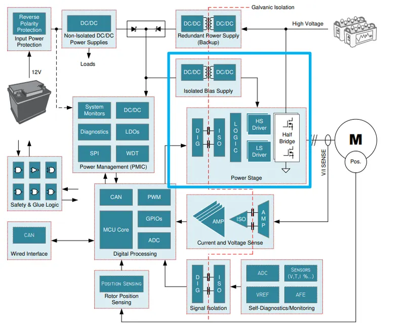
Figure 1 shows a traction inverter reference diagram where the position of the TIDA-020030 is highlighted.
The isolated bias supply and the isolated gate drivers galvanically isolate the high-voltage power switches
from the low-voltage control signals. Each isolated gate driver requires a pair of positive-supply and
negative-supply rails to fully turn on and off the IGBT or SIC power modules.
Figure 1. HEV/EV Traction Inverter Reference Block Diagram and the Position of the TIDA-020030
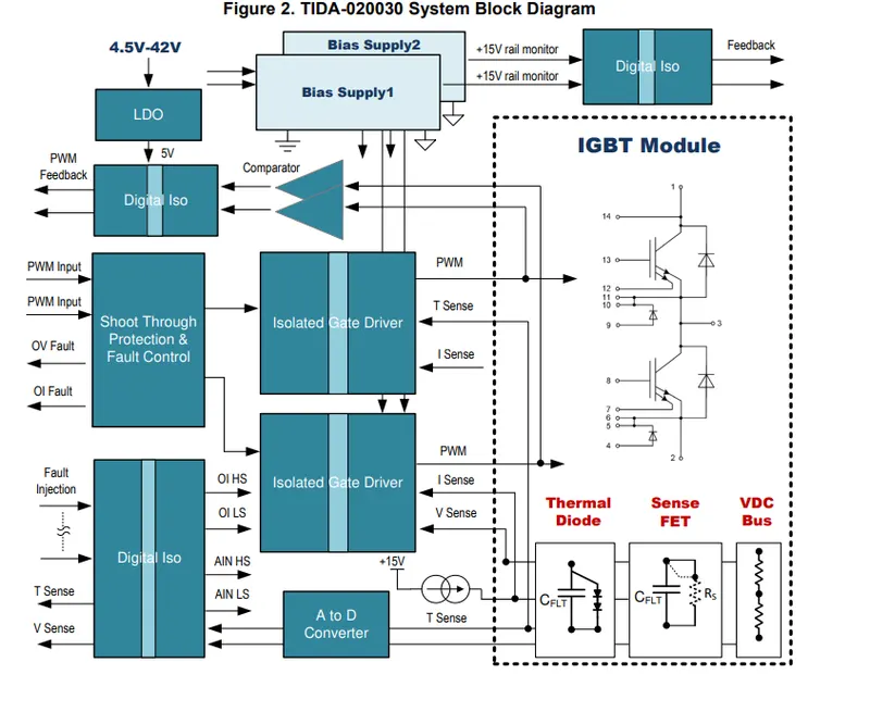
Block Diagram
The TIDA-020030 design drives a double-side-cooled IGBT power module with integrated thermal diode
for temperature sensing and current sensing FET for overcurrent protection. The power stage provides upto-date protection and diagnostic features enabling a high level of safety to the traction inverter system.
The boards consist of the high-side and low-side isolated gate drivers, DC bus voltage sensing, shootthrough protection and fault control, gate drive PWM monitoring, thermal diode sensing circuit, overcurrent
and short-circuit protection, error signal injection channels, and various redundant channels for
protections. The system block diagram is shown in Figure 2. The design includes the following advanced
features for an increased level of safety:
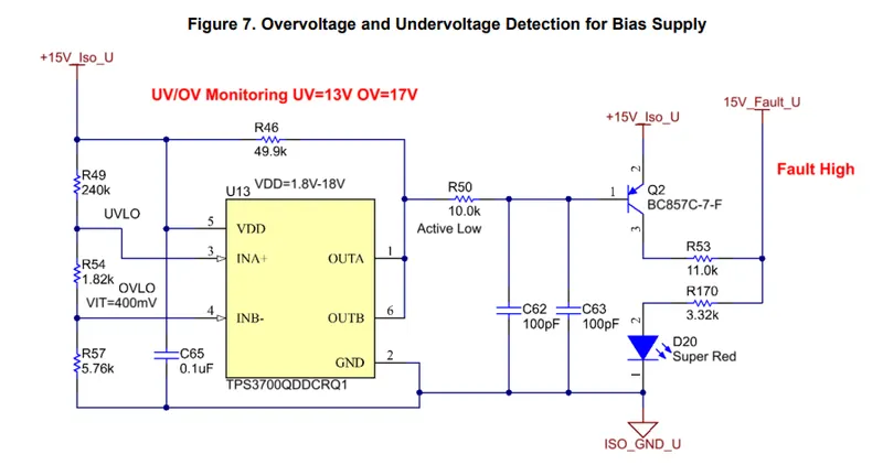
• Undervoltage and overvoltage monitoring on the bias supply rails
• Integrated analog-to-digital converter channel for temperature sensing
• Isolated DC bus voltage sensing path using an isolated amplifier
• Gate PWM comparator for control-signal monitoring
• Fast overcurrent detection through the isolated gate driver analog-to-digital converter
• Thermal diode temperature sensing through a high-side driver and DC bus voltage sensing through a
low-side driver
• Logic shoot-through protection at PWM input
• Redundant sensing paths for increased level of safety:
– DC bus voltage sensing
– Thermal diode sensing
• Fault signal injection for:
– Overcurrent detection on the high side
– Overcurrent detection on the low side
– Isolated analog-to-digital PWM sensor on the high side
– Isolated analog-to-digital PWM sensor on the low side
• Fault signal report to the MCU side:
– PWM gate fault
– Overcurrent from the IGBT module
– Overtemperature from the IGBT module
– DC bus overvoltage
• 4.5-V-42-V input, 15-V - -8-V output, 4.2-W each isolated bias supplies on board
2.2 Design Considerations
The TIDA-020030 reference design features the following Texas Instruments devices.
2.3 Highlighted Products
2.3.1 UCC21732-Q1
The UCC21732-Q1 is a galvanic isolated single-channel gate driver designed for up to 1700-V SiC
MOSFETs and IGBTs with advanced protection features. The UCC21732-Q1 has up to a ±10-A drive
strength and supports up to 1.5-kVRMS working voltage and 12.8-kVPK surge immunity with longer than
40 years of isolation barrier life. The UCC21732-Q1 includes the following state-of-art protection features:
• High (±10-A) drive strength: Eliminates discrete high-current buffers, which are ideal for power
modules, higher system reliability, and lower system cost.
• Fast (650-ns) isolated fault reporting: Faster system protection and shutdown and higher system
reliability.
• Isolated analog-to-digital PWM sensing: Switch temperature sensing, DC bus sensing, auxiliary supply
monitoring, alarm, and so forth.
• Fast (200-ns) overcurrent detection:
– Important for fast-switch protection, especially SiC MOSFETs
– Allows for flexible desaturation (DESAT) threshold setting for SiC MOSFET or IGBT
– Applicable to IGBT modules with SenseFET
• External Miller clamp: Ideal for high-power IGBT/SiC modules (reduces clamp-to-gate parasitics).
• 2-level turnoff: Preferred for high-power modules for higher-power applications.
2.3.2 LM5180-Q1
The LM5180-Q1 device is a primary-side regulated (PSR) flyback converter with high efficiency over a
wide input voltage range of 4.5 V to 70 V. The isolated output voltage is sampled from the primary-side
flyback voltage, eliminating the need for an opto-coupler, voltage reference, or third winding from the
transformer for output voltage regulation. The high level of integration results is a simple, reliable, and
high-density design with only one component crossing the isolation barrier. Boundary conduction mode
(BCM) switching enables a compact magnetic solution and better than ±1% load regulation and line
regulation performance. An integrated 100-V power MOSFET provides output power up to 7 W with
enhanced headroom for line transients.
2.3.3 AMC1311-Q1
The AMC1311-Q1 is a precision, isolated amplifier with an output separated from the input circuitry by an
isolation barrier that is highly resistant to magnetic interference. This barrier is certified to provide
reinforced galvanic isolation of up to 7 kV peak according to VDE V 0884-11 and UL1577. Used in
conjunction with isolated power supplies, this isolated amplifier separates parts of the system that operate
on different common-mode voltage levels and protects lower-voltage parts from damage. The highimpedance input of the AMC1311-Q1 is optimized for connection to high-voltage resistive dividers or other
voltage signal sources with high output resistance.
2.3.4 ADS7049-Q1
The ADS7049-Q1 device is a Q100-qualified, 12-bit, 2-MSPS, analog-to-digital converter (ADC). The
device supports a wide analog input voltage range (2.35 V to 3.6 V) and includes a capacitor-based,
successive-approximation register (SAR) ADC with an inherent sample-and-hold circuit. The SPIcompatible serial interface is controlled by the CS and SCLK signals. The input signal is sampled with the
CS falling edge and SCLK is used for conversion and serial data output. The device supports a wide
digital supply range (1.65 V to 3.6 V), enabling direct interface to a variety of host controllers. The
ADS7049-Q1 complies with the JESD8-7A standard for a normal DVDD range (1.65 V to 1.95 V).
2.4 System Design Theory
2.4.1 Isolated Gate Driver
The schematic of one single-channel, isolated gate driver circuit is shown in Figure 3. The IGBT half
bridge module (FF400R07A01E3_S6) has the integrated thermal diode for temperature sensing and
SenseFET for current sensing and protection. The isolated gate driver circuit is designed with following
considerations:
• Three 5.1-Ohm gate resistors are connected in parallel to ensure high peak current drive and sink to
the IGBT module. The 2010 package with a 0.75-W power rating is used to ensure sufficient heat
dissipation.
• The overcurrent and short-circuit protection function is carried through the OC pin of the UCC21732-
Q1. The current sense FET is connected with a 2-Ohm pulldown resistor. The scale down ratio of the
main loop current and the sensed current through the sensing FET is set as 1:2000.
• A 19-V bidirectional Zener diode is placed close to the IGBT gate for protection.
• A thermal diode output is connected to the analog-to-digital channel input (AIN pin) of the isolated gate
driver. The AD converter encodes the voltage signal VAIN to a PWM signal.
• An external Miller clamp is connected to the IGBT gate through the N-channel MOSFET.
Figure 3. Isolated Gate Driver Circuit With IGBT Module
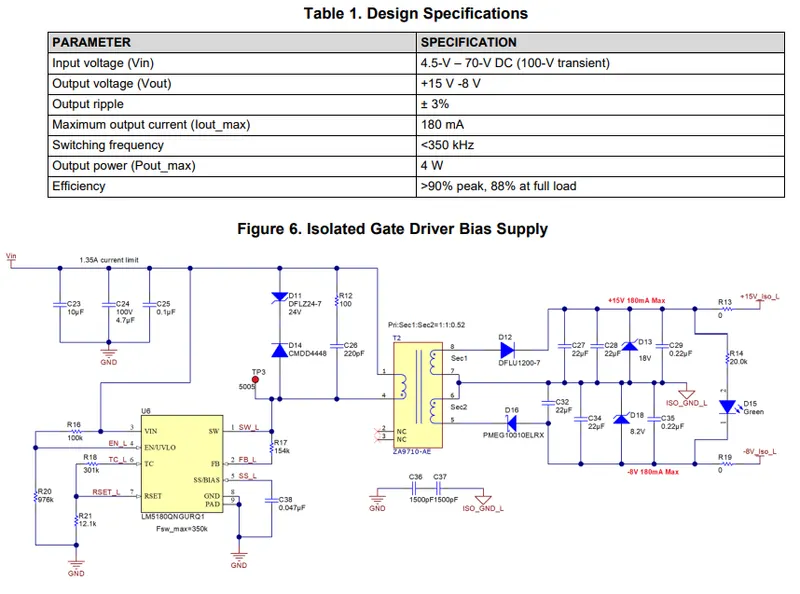
Transformer Design
Key parameters to design the transformer include turns ratio, primary-side inductance, switching
frequency, saturation current, and so forth.
If ignoring the drop voltage across the switching MOSFET, the winding turns ratio is calculated as:
Where:
• VIN-_Min is the minimum input voltage
• Ton is the switch-on time of the switching MOSFET
• Toff is the off time of the switching MOSFET
• NPS is the turns ratio of the transformer
• VD is the output rectification diode (1)
D is the duty cycle, and choosing the maximum duty cycle 75% at minimum input voltage, the turns ratio
of the transformer primary winding to the secondary winding is calculated as:
(2)
Select a magnetizing inductance based on the minimum off-time constraint according to:
Where
• VD is the forward drop voltage of the output rectification diode
• IPRI_PK is the primary winding current when converter operates in frequency foldback mode (1.5 A according to
the data sheet) (3)
The built-in MOSFET of the LM5180-Q1 is rated at 100 V. In the off cycle, when the secondary (flyback)
diode is on, the voltage on the drain (VDS) is calculated as:
Where:
• VIN(MAX) is the maximum input voltage
• IREF is the voltage reflected from the secondary side
• VRING is the excited spike due to resonance (4)
The voltage across the secondary side diode is calculated as:
Where:
• VOUT is the maximum output voltage
• VSPIKE is the excited spike due to resonance (5)
The inductance of the transformer primarily determines the modes of operation in the LM5180 device as
the load is varied from the minimum load to full load. An increase in the magnetic inductance generally
leads to an increase in the leakage inductance of the transformer. The LM5180 device has a minimum offtime (TOFF(MIN)) of 500 ns. The magnetizing current should not decrease to zero in less than 500 ns.
Therefore the minimum primary-side inductance is calculated as:
Where:
• VOUT is the nominal output voltage, which is 24 V
• TOFF(MIN) is the minimum off time of LM5180-Q1
• IPRI_MIN is the minimum peak current flowing at primary side for the LM5180-Q1 which is 0.27 A
• NPS is the primary to secondary turns ratio (6)
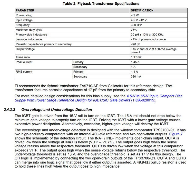
Thus, the designed transformer should have the minimum primary inductance of 30 µH.
Specifications of the designed flyback transformer are summarized in Table 2.
This reference design is an IGBT or SiC isolated gate driver power stage driving a IGBT module with advanced protection features. The design consists of a single phase power stage from a traction inverter supporting high level of safety features. The IGBT module has integrated thermal diode for temperature monitoring and sensing FET for over current protection, providing fast and accurate protections. It includes the bias supplies and its output voltage monitoring, isolated DC bus sensing in redundant circuits, temp sensing for high side and low side drivers, PWM gate signal monitoring, fault signal injection diagnostics. The supply accepts a wide input range of 4.5V to 65V DC, and delivers up to 180mA output current. The isolated gate driver has up to ±10A drive strength and also includes an analog to PWM converter, which is utilized for temperature and voltage sensing.
Features
- Single-phase power stage design for HEV/EV traction inverter applications
- Includes a 700-V, 450-A, double-side-cooled IGBT module with integrated thermal diode for temperature monitoring and sensing FET for overcurrent protection
- Multiple redundant circuits, supply voltage monitoring and PWM output monitoring for increased level of system safety
- Isolated gate driver on board with a ±10-A drive strength, fast overcurrent and short-circuit protection and analog-to-PWM sensor
- Fault signal injection for function validation
2. How do you calculate the trace width, via size and trace length.
Ans:-
Table of Bittele production minimum sizes
| Copper Weight | 0.5oz | 1oz | 2oz | 3oz | 4oz or above | |
| Outer layers | Minimum Trace Width | 3mil | 4mil | 5mil | 6mil | RFQ |
| Minimum Trace Spacing | 4mil | 5mil | 7mil | 10mil | RFQ | |
| Via holes to other copper feature | 7mil | 9mil | 12mil | 16mil | RFQ | |
| Inner layers | Minimum Trace Width | 3mil | 3.5mil | 5mil | 6mil | RFQ |
| Minimum Trace Spacing | 3mil | 4mil | 6mil | 9mil | RFQ | |
| Via holes to other copper feature | 7mil | 8mil | 11mil | 15mil | RFQ |
Notes:
The formula for calculating allowable current through a trace is published in the IPC-2221 standard section 6.2 as shown below.
Internal traces : I = 0.024 x dT0.44 x A0.725
External traces: I = 0.048 x dT0.44 x A0.725
Where I is maximum current in Amps, k is a constant, dT is temperature rise above ambient in °C, & A is cross sectional area of trace mils².
The trace width can then be calculated by re-arranging this formula to determine the cross-sectional area that our desired current can safely pass through.
Area[mils^2] = (Current[Amps]/(k*(Temp_Rise[deg. C])^ 0.44))^(1/0.725)
Then, the Width is calculated from the cross sectional area for a chosen thickness:
Width[mils] = Area[mils^2]/(Thickness[oz]*1.378[mils/oz])
As per IPC-2221 for internal layers k = 0.024 and for external layers: k = 0.048
Disclaimer:
These calculations are industry standard and believed to be correct, but not guaranteed. May not be appropriate for all designs.
3 Q.
Ans:-
How to prevent your PCB from overheating
3 minutes | 27 Jun 2018
PCB Materials for Engineers Explained
Printed circuit board (PCB) materials are formulated to withstand a certain amount of heat. What happens when the temperatures rise beyond certain limits? Performance takes a nose dive, especially at higher frequencies. This is why cost-effective heat management is perhaps an engineer’s number-one priority.
Of course, heat-tolerant PCB materials and carefully designed circuits can tolerate a certain amount of heat. First, the circuit designer should understand the different parameters of the materials’ behaviour when temperatures rise.
See how our range of PCB hardware can help
Heat comes from various sources
Circuit boards are assembled in increasing density to make smaller, lighter designs. A component mounted to the circuit board can produce heat – so can an external source, such as found in automotive electronic systems.
Heat causes most materials to expand
Because of the smaller wavelengths at higher-frequencies, microwave and especially millimetre-wave (30 GHz and higher) circuits have small features that can become distorted as a circuit board expands due to heat.
Adding to this problem is the demand for more compact electronic designs. It’s common to see circuits designed with materials that have higher dielectric constants with smaller circuit features for a particular frequency and wavelength.
When the temperature rises, the circuit materials expand, changing the form of transmission lines and altering the impedance of conductors from a desired value. The results? Loss of linearity, distortion and shifts in frequency because of changes in transmission-line dimensions.
Materials expand at different rates
Circuit boards are made of composite materials, including dielectric layers and conductive metal layers. These composite materials tend to expand at different rates and to different extremes.
The coefficient of thermal expansion (CTE) describes the amount of expansion a material experiences. In an ideal world, the CTE of your board’s dielectric layers are close in value to the copper or other conductive metals laminated to the dielectric materials. Then both materials expand together at high temperatures.
What are your options?
You have several. First, a few points to consider:
- The resistance of copper traces and vias account for significant power loss and heat generation
- Electrical connections with a larger cross-sectional area have lower resistance, which reduces the amount of power lost to heat.
Most PCBs use copper to the equivalent of about 1 ounce per square foot. If using fans or heat sinks are out of the question, a PCB with high current should use at least double this amount of copper. If your circuits operate at over 10 amps, then go as high as 3 or 4 ounces per square foot.
What does heavier copper mean for the width of traces?
You’ll have to increase them. This doesn’t mean losing usable area, however. Place the traces deeper into the board. The heat will dissipate into the board itself and into nearby thermal vias.
Yes, this will probably mean use a thicker board, but that’s a good thing in high-current devices. With thin boards, everything can heat up to a high temperature.
A thicker board requires more thermal energy to reach a high temperature. This helps keep the temperature low at the top of the board.
Consider heat pipe integration
This is especially helpful when your application is a compact electronic device, such as a mobile. This cost-effective, reliable method of passive heat transfer gives you effective thermal conductivity, vibration-free operation and no moving parts.
The pipe contains a small amount of fluid, which can be water, nitrogen, acetone, sodium or ammonia. The fluid absorbs the heat. The resulting vapor then travels along the heat pipe to a condenser region and condenses back into a liquid.
Use thermal interface materials (TIM)
Thermal interface material fills the gaps between surfaces with a substance that offers better thermal conductivity than the air that would otherwise fill those microscopic gaps. In turn, this improve heat transfer between the two surfaces.
Typical TIMs conduct heat around 100 times better than the air they displace. Thermal greases are the favoured material in the electronics sector for improving the performance of the heat sink.
Best of all: active cooling integration
Don’t think just because your application is compact that you can’t use a fan. Micro fans are the most effective way to cool any mobile device. In fact, cooling fans are always your best option, no matter what the size or voltage for your application.
If you’re concerned about the noise fans can produce, you needn’t be. The amount of noise generated is determined by the fan’s size and how fast it spins. The faster, the noisier. But fans can be altered, such as insulating the duct, installing sound-dampening material or simply mounting the fan with soft materials, such as rubber.
Discover our range of PCB LED Mounting Hardware, PCB Mounting Block, PCB Mounting feet, PCB Mounting Pillars, PCB Spacers, PCB Supports and Screw Grommets that can help with preventing the PCB in your application from overheating.
Key Advantages of a 4-Layer PCB
Owing to their beneficial features, 4-layer PCBs are widely used in many electronic applications. Some key benefits offered by these multilayered PCBs are as follows:
- Smaller and Quality-Driven Designs: This is one of the important reasons for using a 4-layer PCB. Owing to their multilayer design structure, they are inherently small in size than single-sided printed circuit boards. This is beneficial for modern electronic devices such as smartphones, tablets, and laptops. As it is a multilayered design, it requires a thoroughly planned design and precision, when mounting components. This helps in reducing unwanted errors and ensures high-quality results.
- Excellent Durability: As described above, these circuit boards not only withstand their weight but also handle applied pressure and heat that bind them together. Additionally, owing to the multiple layers of insulation between circuit layers, their durability increases.
- Higher Assembly Density: These printed circuit boards increase the assembly density by incorporating several layers into one single board. The interconnection between close quarters allows circuit boards to be more connective.
- Lightweight Construction: In a 4-layer PCB, multiple connectors are required to interlink or connect separate single, as well as double-layered circuit boards. It helps in simplifying the circuit design, and reduces its weight.
Applications of a 4-Layer PCB
The key advantages of these circuit boards contribute to their popularity across diverse industries. Following are some important applications where these circuit boards are widely used:
- Heart Monitors
- Computers
- GPS Technology
- File servers
- Mobile Phones
- Data storage
- Signal transmission
- Weather analysis
- Space probe equipment
- X-Ray Equipment
- Atomic accelerators
- Cat scan technology
- Fiber optic receptors
- Central fire alarm systems
- Cell phone transmission and repeaters