Project 2 - Patient monitoring system Design - PCB Design and Mechanical Design part
A Patient Monitoring System (PMS) is a critical component in healthcare that allows continuous or periodic monitoring of a patient's vital signs and other health parameters. Designing such a system involves both electronic (PCB design) and mechanical aspects.A Patient Monitoring System (PMS) is a crucial component of healthcare technology that involves the continuous or periodic observation of a patient's physiological parameters. This monitoring is essential for timely diagnosis, treatment, and management of various medical conditions. Integrating PCB (Printed Circuit Board) design and mechanical design is crucial in developing a reliable and efficient Patient Monitoring System. Here's an explanation of how these two aspects contribute to the overall design:
PCB Design:
- Components Selection: Choose suitable sensors for monitoring vital signs such as heart rate, blood pressure, temperature, and oxygen saturation. Select appropriate microcontrollers, amplifiers, analog-to-digital converters (ADCs), and communication modules.
- Sensor Integration: Integrate sensors onto the PCB to ensure accurate measurement and reliable data acquisition. Proper isolation and noise reduction techniques should be implemented to enhance signal quality.
- Power Management: Design an efficient power supply system with battery backup to ensure continuous monitoring, especially during power outages. Implement power-saving features to extend battery life.
- Data Processing and Storage: Develop a processing unit to analyze and process the sensor data. Include memory components for data storage and retrieval. Implement algorithms for real-time analysis and anomaly detection.
- Communication Interface: Integrate communication modules (such as Wi-Fi, Bluetooth, or cellular) to transmit data to a central monitoring station or a mobile device. Ensure data security and privacy through encryption techniques.
- User Interface: Incorporate a user-friendly interface for healthcare professionals and patients to view real-time data. This can be an LCD display, touch screen, or indicators for different vital signs.
- Alarm System: Implement an alarm system to alert healthcare providers in case of abnormal vital signs. This may include visual and audible alarms.
Mechanical Design:
- Enclosure Design: Design a compact and ergonomic enclosure to house the PCB and other components securely. The enclosure should be durable, lightweight, and easy to clean to meet healthcare standards.
- Sensor Placement: Ensure proper placement of sensors on the device for optimal data accuracy and patient comfort. Consider the anatomical and physiological factors when deciding sensor locations.
- Battery Compartment: Design a compartment to securely hold the battery, considering easy access for replacement or recharging. Implement a mechanism for battery status indication.
- Strap or Mounting System: Include a comfortable and adjustable strap or mounting system for securing the device to the patient. It should be adjustable for different body sizes and easily removable for cleaning.
- Water Resistance: Depending on the use case, consider making the device water-resistant or waterproof to withstand potential exposure to liquids and facilitate easy cleaning.
- Ventilation: Provide adequate ventilation to prevent overheating of electronic components. This is crucial for the device's reliability and safety.
Integration:
- Ensure seamless integration between the PCB and mechanical components, considering factors such as ease of assembly, serviceability, and overall system reliability.
- Conduct thorough testing and validation to ensure the system's functionality, accuracy, and safety.
By combining a well-designed PCB with appropriate sensors and a robust mechanical design, a Patient Monitoring System can offer reliable and accurate health monitoring for patients in various healthcare settings.
Designing a patient monitoring system involves integrating various components, including sensors, microcontrollers, communication modules, and mechanical elements. Here's a general outline of how you might approach the PCB design and mechanical design for such a system:
PCB Design:
System Architecture:
- Define the overall architecture of the patient monitoring system, including the types of sensors (e.g., ECG, temperature, blood pressure) and communication modules (e.g., Bluetooth, Wi-Fi) you plan to use.
Component Selection:
- Choose appropriate sensors, microcontrollers, communication modules, and power management components based on the system requirements.
Schematic Design:
- Create a schematic diagram that illustrates how the selected components are connected. Pay attention to signal conditioning, filtering, and power distribution.
PCB Layout:
- Use PCB design software to lay out the components on the board, considering factors like signal integrity, power distribution, and thermal management. Ensure proper grounding and keep traces as short as possible.
Power Supply Design:
- Design a stable power supply system with the required voltage levels and low noise. Include voltage regulators, filters, and protection circuits.
Signal Integrity:
- Consider the impedance matching and signal integrity of critical analog signals, such as those from sensors like ECG electrodes.
EMC/EMI Considerations:
- Implement techniques to reduce electromagnetic interference (EMI) and ensure electromagnetic compatibility (EMC) with other devices.
Prototyping:
- Create a prototype of the PCB for testing and validation. Iteratively refine the design based on testing results.
Mechanical Design:
Enclosure Design:
- Select or design an enclosure that accommodates the PCB, sensors, and other components. Consider the material, size, and shape for optimal functionality and aesthetics.
User Interface:
- Integrate a user interface into the mechanical design. This could include a display screen, buttons, and indicators for user interaction.
Sensor Placement:
- Plan the placement of sensors on the patient's body or on the device itself for accurate and comfortable monitoring.
Battery Compartment:
- If the system uses batteries, design a compartment within the enclosure for easy access and replacement.
Cable Management:
- Plan for cable routing and management within the enclosure to minimize clutter and prevent interference with the sensors.
Durability and Safety:
- Ensure that the enclosure is durable, safe, and meets relevant standards for medical devices.
Ventilation and Heat Dissipation:
- Incorporate ventilation and heat dissipation mechanisms to prevent overheating, especially if the device operates continuously.
Assembly and Disassembly:
- Design the enclosure to facilitate easy assembly and disassembly for maintenance and potential upgrades.
Prototyping and Testing:
- Create a physical prototype of the device for testing and validation. Ensure that the mechanical design meets functional and usability requirements.
Remember that both PCB and mechanical design are iterative processes, and continuous testing and refinement are essential to achieving a reliable and user-friendly patient monitoring system. Additionally, compliance with relevant medical device regulations and standards is crucial for ensuring the safety and effectiveness of the system.
Designing a patient monitoring system involves both electronics (PCB design) and mechanical design aspects. Below are the key deliverables and considerations for each aspect:
Electronics (PCB) Design:
Understanding of Complete Electronics Subsystem Design Requirements:
- Define the requirements for vital sign monitoring (e.g., ECG, blood pressure, temperature).
- Specify sensor types, signal conditioning, and data acquisition requirements.
- Consider power supply requirements for the system.
Electromechanical System Integration and Challenges:
- Ensure seamless integration of electronics and mechanical components.
- Address challenges such as electromagnetic interference (EMI) affecting sensor data.
- Consider cable routing and connector placement to avoid interference.
PCB Design Hands-On and Challenges:
- Develop the PCB layout based on the system requirements.
- Address challenges like signal integrity, power distribution, and thermal management.
- Ensure proper grounding to minimize noise in the system.
Familiarity with Tools:
- Utilize PCB design tools like Altium, Eagle, or KiCad.
- Understand simulation tools for signal integrity analysis.
- Familiarity with firmware development tools for microcontroller programming.
Medical Devices Design Understanding and Hands-On:
- Comply with medical device standards and regulations (e.g., ISO 13485).
- Consider safety features and fail-safes in the design.
- Incorporate data security and patient privacy measures.
Mechanical Design:
Understanding of Complete Mechanical Subsystem Design Requirements:**
- Define the form factor and enclosure requirements.
- Specify materials for the enclosure based on medical and regulatory standards.
- Consider ergonomics for user comfort.
Electromechanical System Integration and Challenges:
- Design mechanical interfaces for sensors and connectors.
- Address challenges like heat dissipation and ventilation.
- Consider the impact of mechanical design on overall system performance.
Familiarity with Tools:
- Utilize CAD tools (e.g., SolidWorks, AutoCAD) for 3D modeling.
- Simulate and analyze mechanical stresses and thermal effects.
- Work with prototyping tools for rapid iteration.
Medical Devices Design Understanding and Hands-On:
- Ensure the mechanical design aligns with medical device regulations.
- Incorporate features for easy cleaning and sterilization.
- Consider the impact of design on patient comfort during device usage.
Integration:
Electromechanical System Integration:
- Verify alignment of electronics and mechanical components.
- Perform testing for EMI/EMC compliance.
- Conduct system-level testing to ensure all components work seamlessly together.
Challenges and Troubleshooting:
- Develop a systematic approach for troubleshooting integration issues.
- Address challenges related to component compatibility and communication.
Final System Validation:
- Validate the integrated system against design specifications.
- Perform reliability testing and ensure the system meets safety standards.
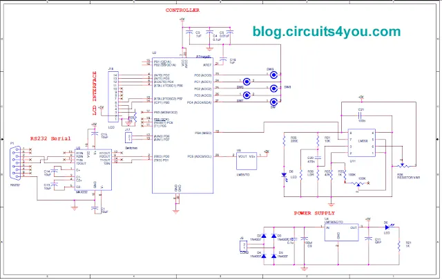
Circuit Design and PCB Manufacturing :
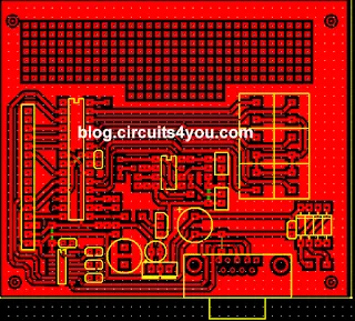
PCB Layout :
There are many portable devices available in market that can measure a single body parameter and keep the records like thermometer. But there is a scarcity of devices that can measure all the body parameters together and continuously monitor them. This system is thus presented with an aimof saving the time of both the doctors as well as patients and hence a number of patients can be observed within a much lesser time. The proposed system has sensors incorporated together to monitor vital signs of human body such as Heart rate, Temperature and Blood pressure. The humanvital body signals which are in analog form are sent to ADC and then to microcontroller. The LCD connected with the microcontroller displays the output of different sensors and simultaneously the output is stored in memory connected with microcontroller.The heart rate is measured with the help of a principle called as photoplethysmography (PPG). The body temperature is measured by using a thermo sensor ,LM35which measures the temperature directly in Fahrenheit and does not need external calibrations. The blood pressure is measured with the help of a pressure sensor; the signals from which are conditioned with an instrumentation amplifier before data conversion by an ADC. Thus, with the help of microcontroller, we can give multiple inputs in the form of body parameters and outputs depending upon the inputs can display the necessary results on LCD.
The proposed system is developed on the integration of hardware as well as software. Fig 1given below shows thegeneralized block diagram of the system.
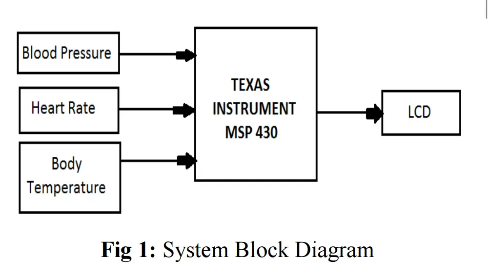
MSP430 Microcontroller
MSP430 Microcontrollers (MCUs) from Texas Instruments (TI) are 16-bit, RISC-based, mixed-signal processors designed specifically for ultra-low-power (ULP). It is based on Von Neuman architecture.MSP430 MCUs have the right mix of intelligent peripherals, ease of use, low cost, and lowest power consumption for thousands of applications. TI offers robust design support for the MSP430 MCU platform along with technical documents, training, tools, and software to help designers develop products and release them to market faster
BLOOD PRESSURE MONITOR:
The blood pressure monitor PCB is the technological heart of a cutting-edge device designed to accurately measure and monitor blood pressure. This compact board incorporates a range of sophisticated components, including sensors, microcontrollers, and display drivers, all seamlessly integrated to provide precise measurements and ensure user-friendly operation.
What is Blood Pressure Monitor PCB?
A Blood Pressure Monitor PCB (Printed Circuit Board) is a crucial component of a blood pressure monitor device. It’s like the brain of the device, responsible for controlling and managing the various functions of the monitor. The PCB consists of different electronic components, such as sensors, microprocessors, memory, and display drivers, which work together to measure and display your blood pressure readings accurately. It’s an essential part of the technology that enables you to monitor your blood pressure conveniently and keep track of your health.
Features of Blood Pressure Monitor PCB
1. Analog-to-Digital Converter (ADC): This feature converts the analog blood pressure signal into a digital format, allowing the device to process the data accurately.
2. Microcontroller Unit (MCU): The MCU acts as the brain of the blood pressure monitor, controlling and coordinating various functions. It manages data processing, user interfaces, and communication with other components.
3. Memory: The PCB may include memory chips to store data, such as previous blood pressure readings or user preferences.
4. Display: A Blood Pressure Monitor PCB often incorporates an LCD or OLED display to provide real-time readings, user prompts, and visual feedback.
5. Pressure Sensor Interface: The PCB includes an interface to connect and communicate with the pressure sensor. This sensor measures the pressure exerted on the cuff during blood pressure measurements.
6. Communication Interfaces: These interfaces enable data transfer and connectivity options, such as USB, Bluetooth, or Wi-Fi. They allow users to upload data to mobile apps or share it with healthcare professionals.
7. Power Management: The PCB includes power management circuitry to regulate the power supply and ensure efficient energy consumption. It may also support battery charging functionality.
8. User Interface: The PCB may incorporate buttons, switches, or touch sensors to provide user input options and control the device’s functions effectively.
9. ESD Protection: To safeguard the circuitry from electrostatic discharge, the PCB includes protective components to prevent damage to sensitive electronics.
Functions of Blood Pressure Monitor PCB
1. Sensor Interface: The PCB connects to the blood pressure sensor and reads the analog signals coming from it. It then amplifies and conditions these signals for further processing.
2. Signal Processing: The PCB processes the amplified signals using analog and digital components. It filters out noise, separates systolic and diastolic pressure values, and calculates pulse rate and other parameters.
3. Display and User Interface: The PCB connects to the display module, which shows the measured blood pressure values and other relevant information. It also handles user input from buttons or touch panels, allowing users to navigate through the device’s menu.
4. Memory and Storage: Some blood pressure monitors include PCBs with memory components, enabling them to store previous measurements. This allows users to track their blood pressure over time and share the data with healthcare professionals if needed.
5. Power Management: The PCB regulates the power supply for different components of the blood pressure monitor, ensuring optimal performance and energy efficiency. It may also include battery charging circuitry for devices with rechargeable batteries.
6. Communication: In advanced blood pressure monitors, the PCB might incorporate communication modules like Bluetooth or Wi-Fi, which enable data transfer to smartphones or other devices for further analysis or remote monitoring.
Applications of Blood Pressure Monitor PCB
1. Personal Health Monitoring: The PCB can be integrated into wearable devices, allowing individuals to continuously monitor their blood pressure throughout the day. This helps in keeping track of their health and detecting any potential issues.
2. Hospital and Clinical Settings: Blood Pressure Monitor PCBs are commonly used in hospitals and clinics to accurately measure patients’ blood pressure. They are found in both stationary and portable devices, enabling healthcare professionals to monitor patients’ vital signs and make informed decisions about their treatment.
3. Health and Fitness Wearables: Many fitness enthusiasts use wearable devices, such as smartwatches and fitness bands, to track their activities. With the inclusion of a Blood Pressure Monitor PCB, these devices can provide users with real-time blood pressure data, helping them understand the impact of their workouts on their cardiovascular health.
4. Remote Patient Monitoring: Blood Pressure Monitor PCBs play a crucial role in remote patient monitoring systems. Patients can measure their blood pressure at home using specialized devices with integrated PCBs. The data is then sent to healthcare providers for analysis, allowing them to remotely monitor patients’ conditions and provide appropriate medical advice.
5. Research and Development: PCBs are also essential in the development of new medical technologies and devices. Researchers use Blood Pressure Monitor PCBs to experiment with different measurement techniques, analyze data, and improve the accuracy and reliability of blood pressure monitoring systems.
IBE’s Capabilities on Blood Pressure Monitor PCB
– Customizable design and dimensions
– High-quality materials and components
– Advanced manufacturing processes and equipment
– Strict quality control and testing procedures
– Fast turnaround time and on-time delivery
HEARTBEAT SENSOR :
The Heartbeat Sensor PCB is an essential component used in medical devices to monitor and detect a person’s heartbeat. It is a small, electronic board that enables the accurate measurement of the heart’s electrical signals. The PCB acts as the central hub, connecting various sensors, amplifiers, and filters that work together to capture the electrical activity of the heart. These signals are then processed and analyzed to provide valuable information about a person’s heart rate and rhythm.
What is Heartbeat Sensor PCB?
The Heartbeat Sensor PCB is a printed circuit board (PCB) used in medical devices to measure and monitor a person’s heartbeat. It is designed to detect the electrical signals produced by the heart and convert them into a digital format that can be interpreted by other components in the device. This allows healthcare professionals to monitor a patient’s heart rate and rhythm, helping to diagnose and treat various cardiac conditions. The Heartbeat Sensor PCB plays a vital role in ensuring accurate and reliable heart rate monitoring.
Features of Heartbeat Sensor PCB
1. Sensor Module: The PCB contains a specialized sensor module that accurately detects the user’s heartbeat. It typically uses infrared light to measure blood flow and detect pulsations.
2. Microcontroller: The PCB is equipped with a powerful microcontroller that processes the signals received from the sensor module. It performs calculations and analyses to accurately determine the user’s heart rate.
3. Analog-to-Digital Converter (ADC): The ADC is an essential component that converts the analog signal from the sensor module into a digital format that can be processed by the microcontroller. This conversion ensures accurate measurement of the heartbeat.
4. Signal Filtering and Amplification: The PCB incorporates various filters and amplifiers to remove noise and enhance signal quality. This helps to improve the accuracy and reliability of the heartbeat measurements.
5. Output Interface: The PCB often includes an output interface, such as a display or LED indicators, to present the user’s heart rate in a user-friendly manner. This allows users to conveniently monitor their heart rate in real time.
6. Power Management: Efficient power management circuitry is integrated into the PCB to optimize energy consumption. This ensures longer battery life and enables the sensor to be used continuously without frequent recharging or replacement.
7. Connectivity Options: Some advanced versions of the Heartbeat Sensor PCB may come with connectivity options like Bluetooth or Wi-Fi. This allows users to connect the sensor to external devices, such as smartphones or smartwatches, for real-time data tracking and analysis.
Functions of Heartbeat Sensor PCB
1. Heart rate measurement: The PCB detects electrical signals from the heart through sensors placed on the body. It then converts these signals into digital data, allowing for accurate heart rate measurements.
2. Signal amplification: The PCB amplifies the weak electrical signals from the heart to ensure reliable and precise readings. This amplification process helps enhance the signal quality, especially in situations where the heart’s electrical activity may be faint.
3. Filtering and noise reduction: To obtain clean and accurate data, the PCB employs filters to reduce noise and unwanted interference from surrounding electrical signals. This helps eliminate any disturbances that could affect the accuracy of the heart rate measurement.
4. Signal processing: The PCB includes microcontrollers or digital signal processors to analyze and process heart rate data. It performs calculations, such as detecting the peak of each heartbeat, determining the pulse rate, and even providing additional features like calculating average heart rate over time.
5. Communication: Depending on the design, the Heartbeat Sensor PCB can facilitate communication with other devices like smartphones or fitness trackers. This enables seamless transfer of heart rate data, allowing users to monitor their heart health, track workouts, or even receive alerts in case of abnormal heart rate patterns.
Applications of Heartbeat Sensor PCB
1. Health and Fitness Monitoring: The heartbeat sensor PCB can be used in wearable devices like fitness trackers or smartwatches to monitor your heart rate during activities and workouts. It can provide valuable insights into your overall health and help you track your fitness progress.
2. Medical Monitoring: Hospitals and clinics can use heartbeat sensor PCBs for patient monitoring during surgeries, post-operative care, or in intensive care units. The sensor can provide real-time data on a patient’s heart rate, allowing medical professionals to closely monitor their condition and make informed decisions.
3. Stress Management: Heartbeat sensor PCBs can be incorporated into stress management devices or apps. By measuring heart rate variability, these devices can provide feedback on the user’s stress levels, helping them practice relaxation techniques and maintain a healthy emotional state.
4. Sleep Tracking: Heartbeat sensor PCBs can be integrated into sleep tracking devices, enabling them to monitor the user’s heart rate during sleep. This can provide insights into sleep quality, detect any irregularities, and help individuals optimize their sleep patterns for better overall health.
5. Gaming and Virtual Reality: Heartbeat sensor PCBs can add an immersive element to gaming or virtual reality experiences. By tracking the user’s heart rate, game dynamics can be adjusted based on their level of excitement or engagement, creating a more personalized and interactive gaming experience.
IBE’s Capabilities on Heartbeat Sensor PCB
– Customizable design and dimensions
– High-quality materials and components
– Advanced manufacturing processes and equipment
– Strict quality control and testing procedures
– Fast turnaround time and on-time delivery
Body Temperature:
The body parameter, body temperature is measured by using a thermo sensor which measures the temperature directly in Fahrenheit and does not need external calibrations.Fig4 below shows the internal configuration and working of the thermo sensor LM35 used in the project.
Fig 4: Internal configuration of LM35There are two transistors in the center of the drawing. One has ten times the emitter area of the other. This means it has one tenth of the current density, since the same current is going through both transistors. This causes a voltage across the resistor R1 that is proportional to the absolute temperature, and is almost linear across the range we care about. The "almost" part is taken care of by a special circuit that straightens out the slightly curved graph of voltage versus temperature. The amplifier at the top ensures that the voltage at the base of the left transistor (Q1) is proportional to absolute temperature by comparing the output of the two transistors. The amplifier at the right converts absolute temperature (measured in Kelvin) into either Fahrenheit or Celsius, depending on the part (LM34 or LM35). Output isthus directly displayed on the LCD.
SYSTEM IMPLEMENTATION
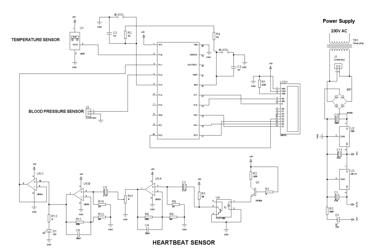
The following figure 5 shows the interfacing of microcontroller MSP 430 with the three specified body parameters viz., blood pressure, body temperature and heart beats. The results so obtained are displayed on the LCD which is interfaced with MSP 430
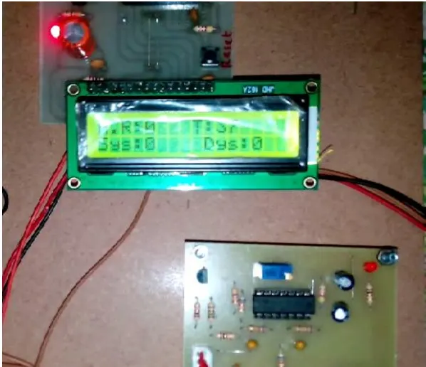
After completing all the processes like PCB designing, etching and soldering, the proposed system was thus finally practically implemented as shown in the fig below
ADVANTAGES
- Real time support for improved health outcome and quality of life.
- Provides extension of care at home after discharge helping to prevent emergencies.
- Ability to continue monitoring patient‟s health, regardless of patients location, even when not at home.
- Provides out of hospital remote monitoring of patients to improve patients‟ care and reduced costs.
- More accountability from patients and care provider
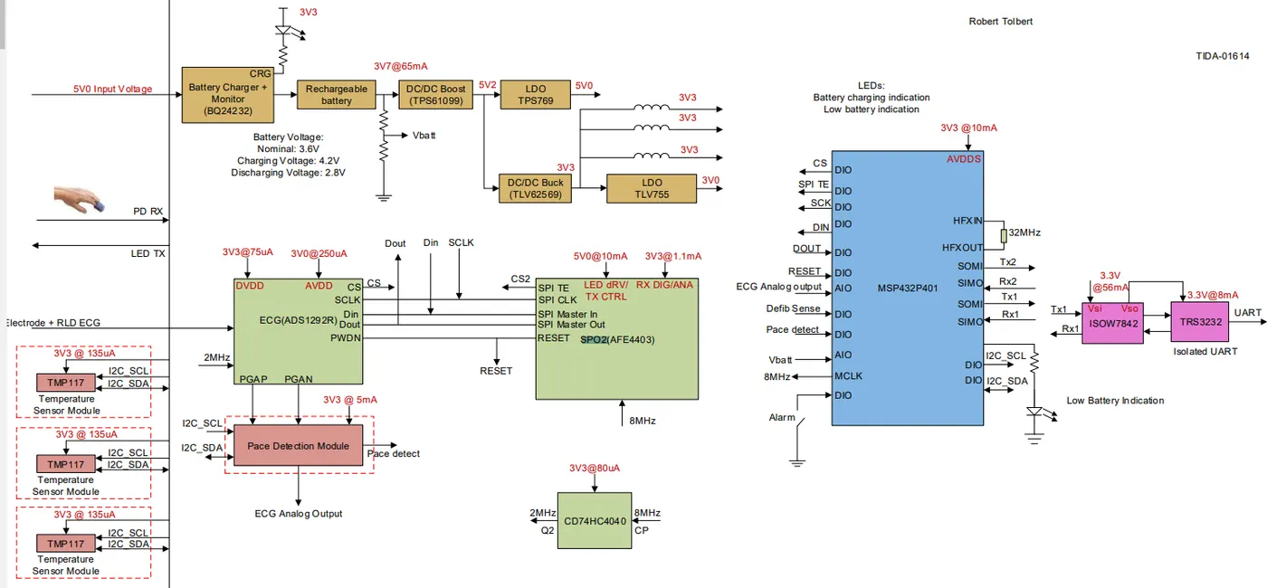
Parameters Measured Using TIDA-01614
In this reference design, five primary vital signs are measured. ECG detects cardiac (heart) abnormalities by measuring the electrical activity generated by the heart as it contracts. ECG measurement uses ECG electrodes that are placed on the chest or at the four extremities (RA = right arm, LA = left arm, RL = right leg, LL = left leg). This reference design measures ECG with a three electrode operation, including the right leg drive, which improves CMRR. ECG is measured using TI’s bio-sensing front-end IC ADS1292R. The ADS1292R is a low-power, multichannel, simultaneously-sampling, 24-bit deltasigma (ΔΣ), analog-todigital converter (ADC) with integrated programmable gain amplifiers (PGAs), internal reference, and an onboard oscillator. This device integrates various ECG-specific functions that support scalable ECG, sports, and fitness applications. The devices is used in high-performance, multichannel data acquisition systems by powering down the ECG-specific circuitry. The ADS1292R has a highly programmable multiplexer that measures temperature, supply, input short, and RLD. Additionally, the multiplexer lets you program any of the input electrodes as the patient reference drive. You can choose the PGA gain from one of seven settings (1, 2, 3, 4, 6, 8, and 12). The ADCs in the device offer data rates from 125 SPS to 8 kSPS. Communication to the device is accomplished through an SPI-compatible interface. The device provides two general-purpose I/O (GPIO) pins for general use. Multiple devices synchronize using the START pin. The internal reference is programmed to either 2.42 V or 4.033 V. The internal oscillator generates a 512-kHz clock. The versatile right leg drive (RLD) block lets you choose the average of any combination of electrodes to generate the patient drive signal. Lead-off detection is accomplished either by an external pullup or pulldown resistor or the internal current source or sink from the device. An internal AC lead-off detection feature is available. The ADS1292R version also includes a fully-integrated respiration impedance measurement function. See the Low-power, 2-channel, 24-bit analog front-end for biopotential measurements data sheet for further details. The ECG subcircuit is implemented with the ADS1292R IC. The ADS1292R is clocked either by an internal oscillator that generates a 512-kHz clock, or externally through the CLK pin (pin 17). Each clocking method has its advantages and disadvantages. Although the external clock provides high accuracy, it requires additional external components. However, the internal clock requires fewer components, but it suffers from temperature-dependent performance. As mentioned in the data sheet, internal clocking is ideal for low-power, battery-operated systems. The internal oscillator is trimmed for accuracy at room temperature. The accuracy varies over the specified temperature range. The only permissible external clock frequencies are 512 kHz or 2.048 MHz. The higher frequency option helps the SPI run at a higher speed. The ADS1292R uses the SPI communication interface to communicate with a Microcontroller (MCU), MPU, or DSP.
SPO2 Monitoring
Oxygen binds to hemoglobin in red blood cells as it moves through the lungs. It travels throughout the body as arterial blood. A pulse oximeter uses two light frequencies (red and infrared) to determine what percentage of hemoglobin is saturated with oxygen. The percentage is called blood oxygen saturation, or SpO2. It is the percentage of oxygenated hemoglobin (hemoglobin containing oxygen) compared to the total amount of hemoglobin in the blood (oxygenated and non-oxygenated hemoglobin). A pulse oximeter also measures and displays the pulse rate and the SpO2 level simultaneously. The signal obtained from the pulse oximeter is the photoplethysmographic (PPG) signal, which shows the blood flow at the extremities. SpO2 is measured by a pulse oximeter, which is an indirect, non-invasive method. It emits and absorbs a light wave passing through blood vessels (or capillaries) in the fingertip. A variation of the light wave passing through the finger gives the SpO2 measurement since the degree of oxygen saturation causes variations in the blood’s color. This value is represented by a percentage. If your pulse oximeter says 98%, then each red blood cell is made up of 98% oxygenated hemoglobin and 2% non-oxygenated hemoglobin. Normal SpO2 values vary between 95% and 100%. Anything lower than 90% may be a cause for concern. Red and infrared (IR) lights are used to estimate the true hemoglobin oxygen saturation of arterial blood. Oxyhemoglobin (HbO2) absorbs visible and infrared IR light differently than deoxyhemoglobin (Hb), and appears bright red as opposed to the darker brown of Hb. Absorption in the arterial blood is represented by an AC signal that is superimposed on a DC signal, representing absorptions in other substances like pigmentation in tissue, venous, capillary, bone, and so forth. The cardiac-synchronized AC signal is approximately 1% of the DC level. This value is known as the perfusion index percentage. Equation 1 shows how to approximate the ratio of ratios and R: R = (ACrms of Red) / (DC of Red) / (ACrms of IR) / (DC of IR) (1) Equation 2 shows the standard model for computing SpO2: % SpO2 = 110 – (25 × R) (2) This model is often used in medical devices literature. However, accurate % SpO2 is computed based on the empirical calibration of the ratio of ratios for the specific device.
ECG and Respiration Circuit
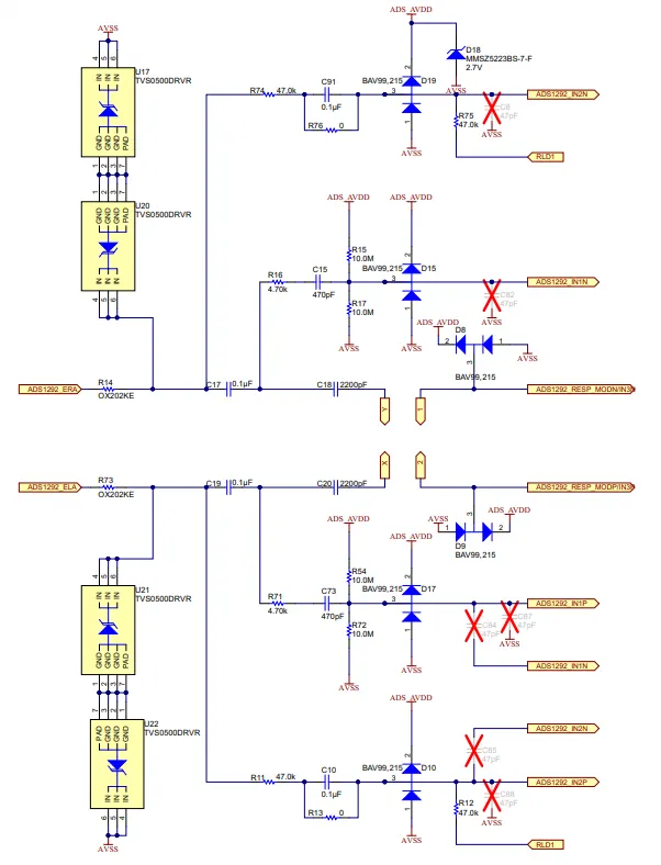
The schematic of the ECG subcircuit and the nets of ADS1292_ERA, ADS1292_ELA, and ADS1292_RLD and corresponds to the probes. The more channels an ECG monitoring system has, the better the ECG signal can be analyzed. ADS1292R is equipped with only two channels. Figure 4 shows that Channel 1 is used for respiration rate calculation and Channel 2 is used for ECG measurement. The frequency from the ECG signals can range from 0.01–300 Hz. ECG drift occurs when the ECG signals drift all over the monitoring device. Current injection and resistor biasing reduce ECG drift, but for added security, the ECG subcircuit uses both methods. resistors R21, R22, R24, R10, and capacitor C16, which form the RLD current injection method. The resistors R15, R17, R54, and R72, which form the resistor biasing method. the ADS1292 decoupling capacitors. ADS1292_ERA ADS1292_ELA C17 0.1µF C18 2200pF ADS1292_RESP_MODN/IN3N 470pF C15 4.70k R16 10.0M R17 10.0M R15 ADS_AVDD AVSS 1 3 2 BAV99,215 D15 ADS1292_IN1N ADS_AVDD AVSS C19 0.1µF C20 2200pF ADS1292_RESP_MODP/IN3P 470pF C73 4.70k R71 10.0M R72 10.0M R54 ADS_AVDD AVSS 1 3 2 BAV99,215 D17 ADS1292_IN1P ADS_AVDD R11 47.0k 0.1µF C10 0R13 1 3 2 BAV99,215 D10 ADS1292_IN2N ADS_AVDD AVSS 47.0k R12 R74 47.0k 0.1µF C91 0R76 1 3 2 BAV99,215 D19 ADS1292_IN2P 2.7V D18 MMSZ5223BS-7-F ADS_AVDD AVSS 47.0k R75 RLD1 RLD1 AVSS AVSS IN 4 IN 5 GND 1 GND 2 IN 6 GND 3 PAD 7 U20 TVS0500DRVR IN 4 IN 5 GND 1 GND 2 IN 6 GND 3 PAD 7 U17 TVS0500DRVR AVSS IN 4 IN 5 GND 1 GND 2 IN 6 GND 3 PAD 7 U21 TVS0500DRVR IN 4 IN 5 GND 1 GND 2 IN 6 GND 3 PAD 7 U22 TVS0500DRVR AVSS R14 OX202KE R73 OX202KE 1 3 2 D8 BAV99,215 AVSS ADS_AVDD 1 3 2 D9 BAV99,215 AVSS ADS_AVDD 47pF C84 ADS1292_IN1N 47pF C85 ADS1292_IN2N 47pF C88 AVSS 47pF C87 AVSS 47pF C82 AVSS 47pF C8 AVSS Y 1 X 2 , Texas Instruments Incorporated Multiparameter Front-End Reference Design for Vital Signs Patient Monitor The ADS1292R is a two-channel device, but if respiration rate detection is enabled, then Channel 1 can no longer measure ECG signals. Four pins are needed to detect the respiration rate: • IN1P • IN1N • RESP_MODP • RESP_MODN The ECG subcircuit can only measure ECG signals, but you can extract the ECG signal respiration rate with mathematical manipulation.
Hardware, Software, Testing Requirements, and Test Results
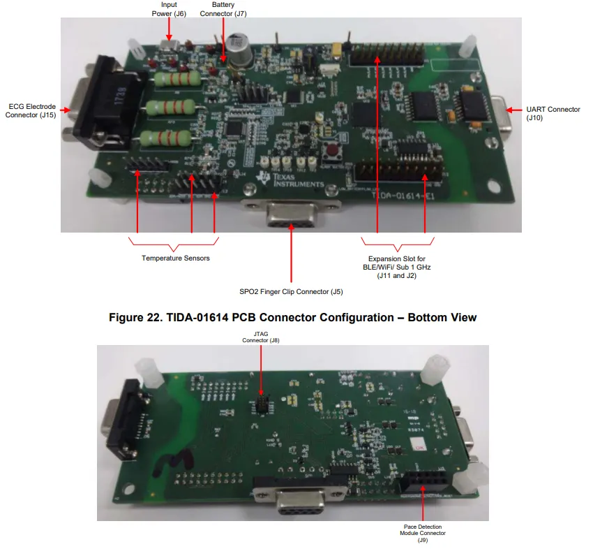
The following list provides information about each part:
- Input Power Connector (J6): A USB-connector for 5-V input power 5 V. 5 V is derived from the USB Vbus.
- Battery Connector (J7): This pin connects the rechargeable 3.7-V Lithium-ion battery.
- UART Connector (J10): This connector is given as a provision to connect to the PC through serial port.
- ECG Electrode Connector (J15): This pin connects the ECG electrodes in 2 electrode and 3 electrode operations.
- Temperature Sensor Connector (J3,J4 and J13): These connectors connect the three temperature sensors.
- SPO2 Finger Clip Connector (J5): This connector connects the SPO2 finger clip.
- Expansion Slot for BLE/WiFi/Sub 1 GHz (J11 and J12): These connectors are the expansion slot for BLE/WiFi/Sub 1 GHz.
- JTAG Connector (J8): The JTAG connector is for programming.
- Pace Detection Module connector (J9): This connector connects the pace detection Module (TIDA010005).
- Isolated UART connector (J16) : This connector is used to give the provision to have 3.3 V isolated UART signals. Connect the USB to UART Dongle (C232HD-DDHSP-0) from this connector to the PC.
Test Setup.
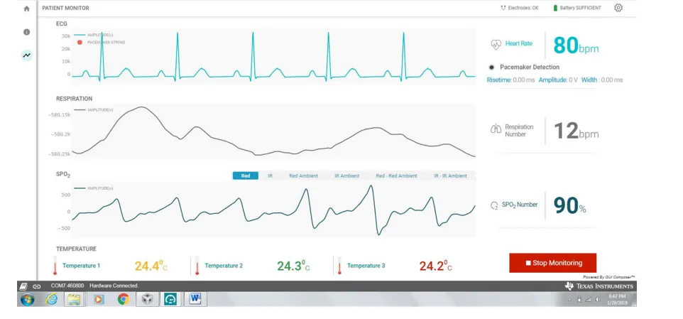
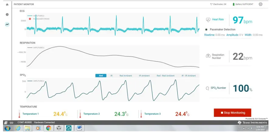
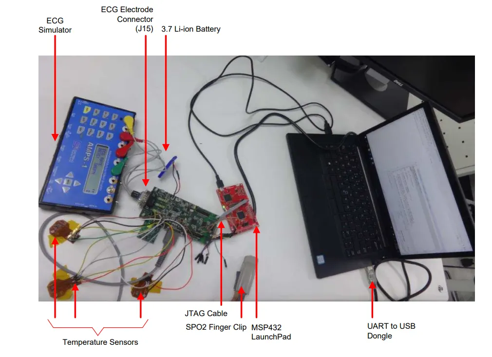
An ECG simulator (Datrend AMPS-1 Advanced Modular Patient Simulator) generates ECG, Respiration, and pace signal for testing. The TIDA-01614 board is programmed using the MSP432 launch pad, connecting to the PC. Three temperature sensor Flex PCBs are connected to this board. Flexi PCB can be easily strapped on to the human board for temperature measurement. Three such temperature sensors are used for accurate temperature measurement. Three ECG electrodes connected to the right arm, left arm, and right leg attach to this board using J15 connector. The system runs with a rechargeable 3.7-V 500 mAh Li-ion battery connected to J7 connector. C232HD – DDHSP-0 UART to USB serial cable is used for UART communication to the PC and GUI.
Test Results :