Project 2
Aim:
Design an interleaving DC/DC converter system for a data centre application
Write up:
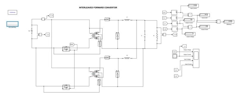
Interleaving DC/DC convertor are a type of topologies which are used to convertor fixed DC voltage to variable DC voltage. One of the advantages of this type of convertor is its high efficiency. An interleaved DC-DC converter uses multiple switching converter stages in parallel connected to an input and output point. Here, step down voltage is required at the output end hence buck conversion can be used. But, the duty ratio required for conversion from `V_(i n) =45V -60V` to `V_(out) = 3V` via buck convertor is too low. This means Direct transfer of energy from source to load is low & hence `eta` will be low. Hence, we will go for forward convertor which uses a transformer in between to take step down & the duty ratio can be nominal. Here, we have assumed `D = 0.5`. The forward convertor consists of a step down transformer between the switch block(MOSFET & diode).
The forward convertor can be realized in two ways:
- With tertiary winding
- Without tertiary winding & with extra switches
Here, forward convertor with tertiary winding is being used. The main use of the tertiary winding is to generate -ve voltage across the magnitizing inductance during the the OFF state of the switch.
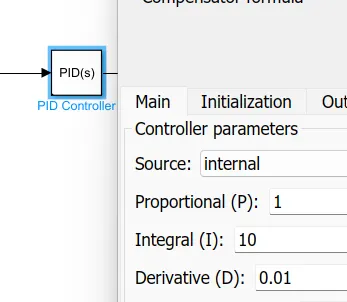
Here, when only one stage of forward convertor was being used, the efficiency was as low as 30%. In order to increase the `eta`, interleaving technique was used. Two forward convertors in parallel were connected & the MOSFETs were given the switching pulses from A PID controller whose parameters are attached below.
Technical inputs available:
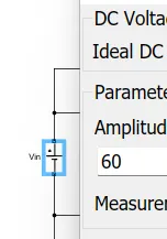
`V_(i n) = 45V-60V`
`V_(out) = 3V`
`I_(out) = 100A`
Requirements:
The efficiency of the system is accepted to be more than 85%.
Assumptions made:
`DeltaI_L = 10% of I_(out)`
`DeltaV_(out) = 1% of V_(out)`
`f_s = 200kHz`
`D = 0.5`
Calculations:
As stated above, Forward convertor is being used for this simulation. The convertor voltage ratio is given by:
`V_(out)/V_(i n) =D.(N_2/N_1)` where N2 & N1 are no of turns of the transformer.
Assuming `V_(i n) = 60V`
`=> N_2/N_1 =1/10`
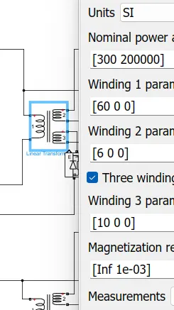
Considering `N_1 = 60`
`:. N_2 = 6`
Now, for complete discharge of magnitizing inductance in one cycle, we would want that Lm to be in discontinous mode.
Hence, `(DT + D_1 T) < T`
`=> D(1+(N_3/N_1))<1`
`=>N_3 < 60`
Lets Assume `N_3 = 6`
Designing the convertor inductor:
We know that, `L = (V_(out)(1-D))/(f_sDeltaI_L`
Here, we are dividing the output current into into parts, i.e `I_(L_1) + I_(L_2) = I_(out)`
So, each inductor will have the current `I_(L_1) = I_(L_2) = 50A`
`=> DeltaI_(L_1) = DeltaI_(L_2) = 0.1 * 50 =5A`
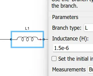
=> `L1 = L2= 1.5muH`
Designing the capacitor:
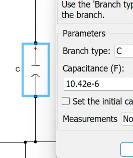
We know that `C_(out) = (1-D)/(8Lf_s^2((DeltaV_(out))/V_(out))` = `10.42muF`
The schematics of the interleaved forward convertor is attached as shown:
Following are the component value taken:
Input Voltage
Transformer:
Inductors:
Capacitor:
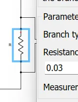
Resistance:
PID control:
Following are the graphs which has been obtained considering all the non idealties of the components:
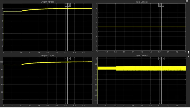
Output voltage:
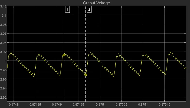
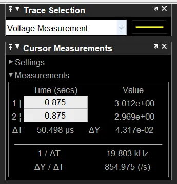
As can be seen, `DeltaV_(out) = 0.043V ~~0.03V` as calculated above
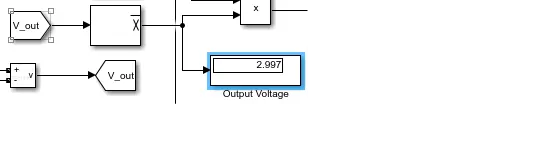
`V_(out_(avg)) = 2.997V`
Output Current:
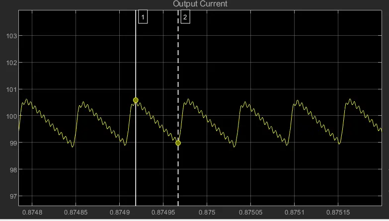
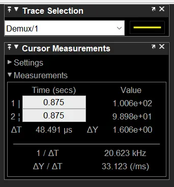
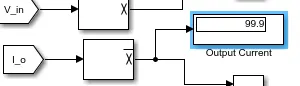
As we can see, `I_(L_(avg)) = 99.9A`
Input Voltage:
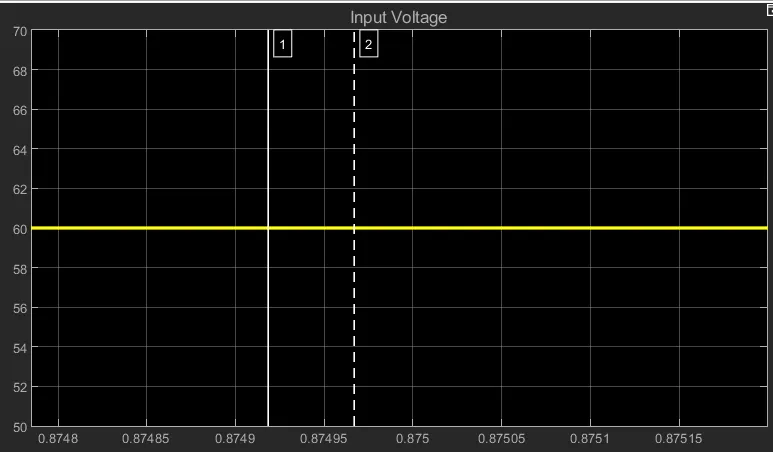
`V_(i n) = 60V`
Input Current:
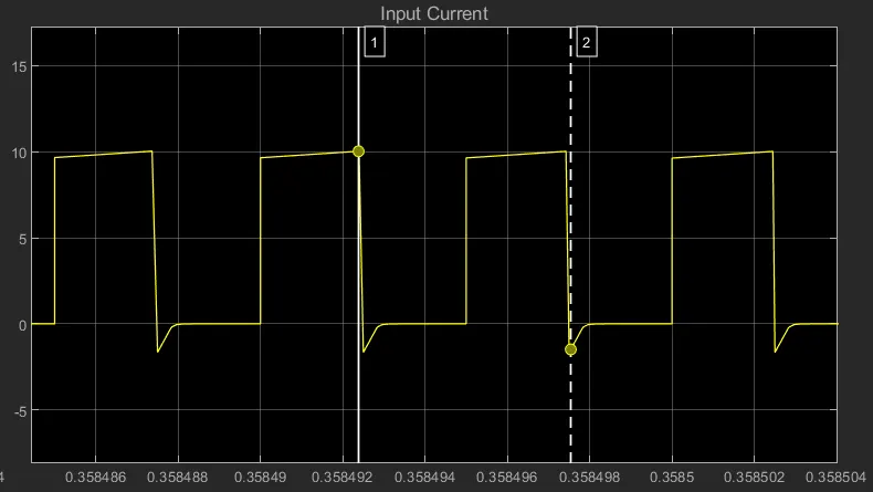
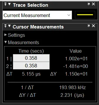
`I_(i n_(min)) = -1.481A`
`I_(i n_(max)) = 10.02A`
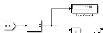
`I_(i n_(avg)) = 5.443A`
Efficiency:
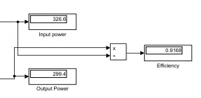
Efficiency of 91% is acheived when considering all the internal resistances & forward voltage drops of switches & non idealities of the components.