Project 1
Aim:
To realize any three topologies in Simulink & obtain the wavforms as per the question regarding the DC DC convertors.
The three topologies choosen here are:
- Buck Convertor in CCM mode
- Inverting Buck-Boost Convertor in CCM mode
- Boost Convertor in CCM mode
Inputs available:
1) Buck Convertor in CCM mode
`40VleV_(i n)le50V`
`V_(out) = 30V`
`P_(out) = 500W`
2) Inverting Buck-Boost Convertor in CCM mode
`30VleV_(i n)le60V`
`V_(out) = -45V`
`P_(out) = 300W`
3) Boost Convertor in CCM mode
`200VleV_(i n)le300V`
`V_(out) = 400V`
`P_(out) = 4kW`
Each of the toplogies are realized on Simulink. The waveforms & the calculations can be found for each one of them.
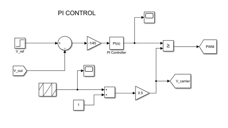
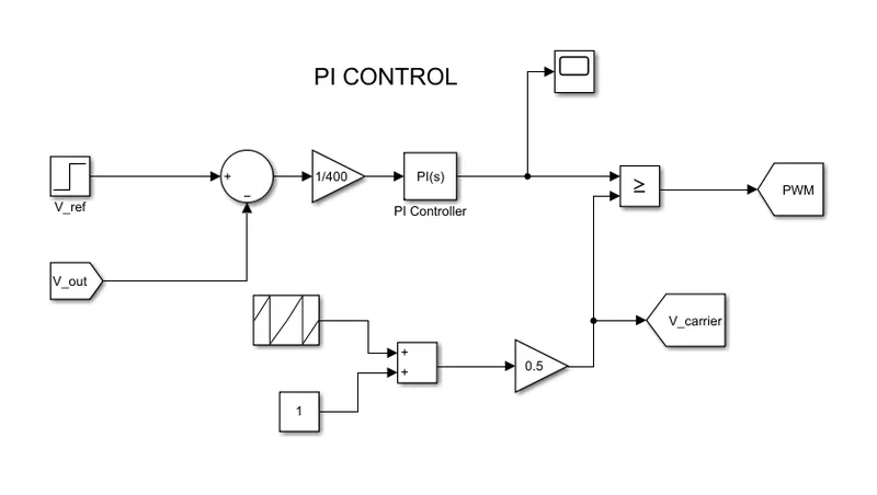
PI control used for close loop to maintain the output voltage
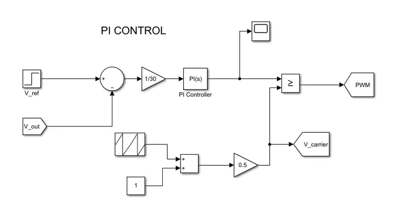
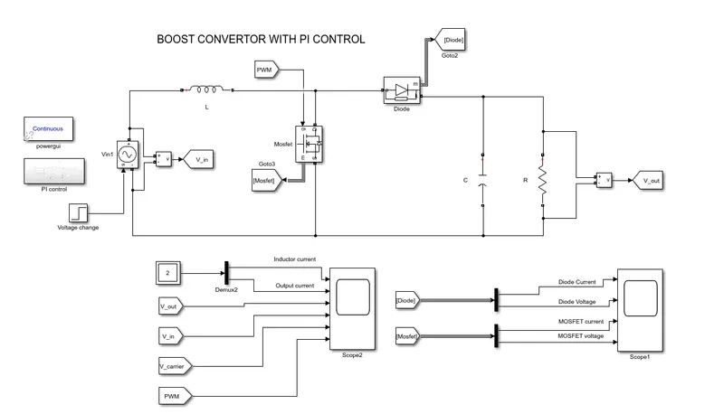
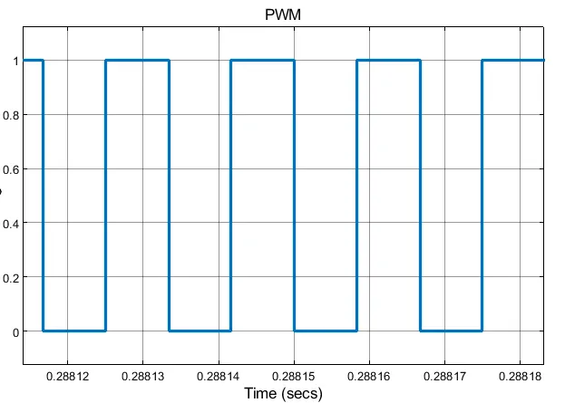
A PI controller is used to maintain the output voltage at the required value. Here the actual output voltage is compared with the refernce voltage(required output voltage). The error is then fed to the PI controller after multiplying with the DC gain of `1/V_(ref)`. The output of the PI controller is then compared with a carrier wave(sawtooth waveform) whose frequency is set at which we expect the MOSFET to turn on & off. The division with `1/V_(ref)`is done so that the comparison with carrier wave, whose magnitude is between 0 to 1, can be done. The PWM signal is generated on the concept that if PI control output is greater than the carrier wave at any point of time, then PWM will be 1 else 0. This PWM is then fed to the MOSFET.
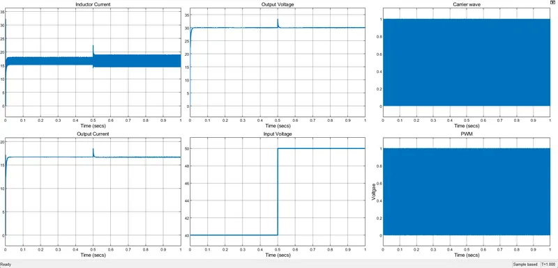
The output voltage is maintained at the required voltage which can be seen in the zoomed out view of the waveforms.
BuckConvertor_withPIcontrol.mdl
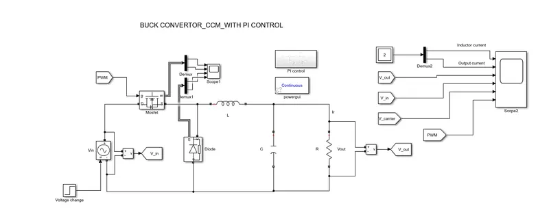
The DC/DC buck convertor converts higher voltage to lower voltage. The Mosfet is a high frequency switching device which turns on & off in a controlled manner depending on the duty cycle which is generated via PI control. The inductor is used to reduce the current ripple caused due to repeated switching. The capacitor has been used to reduce the voltage ripple at the output. The output voltage at resistance has to be maintained constant which is possible when the current through the resistance is constant. This can be possible only when the capacitor absorbs all the ripple hence `I_(L avg )= I_o`& `I_(L rippl e) = I_c`. The diode is used so that when MOSFET turns off, the current flowing through the inductor free wheels through the diode hence preventing high flow of current through MOSFET.
Following are the assumptions made in regards with the schematics:
`DeltaI_L = 30% of I_o`
`f_s = 20kHz`
`DeltaV_(out) = 1% of V_(out)`
Following are the calculations which are done to obtain the component values:
`R = V_(out)^2/P_(out)` = 1.8`Omega`
`I_o = P_(out)/V_(out)` = 16.67A
`I_(L_(avg)) = I_o` = 16.67A`
`D = V_(out)/V_(i n)`
For `V_(i n) = 40V` , D = 0.75
For `V_(i n) = 30V`, D = 0.6
`DeltaI_L =` 5.001A
`DeltaV_(out) =`0.3V
`L = (V_(out)(1-D))/(f_sDeltaI_L)` = 119.976 `muH`
`C_(out) = (1-D)/(8Lf_s^2((DeltaV_(out))/V_(out))` = 96.154`muF` assuming L = 130`muH`
ZOOMED OUT VIEW
ZOOMED IN VIEW
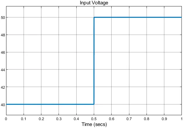
Input Voltage
`40VleV_(i n)le50V`
Output Voltage
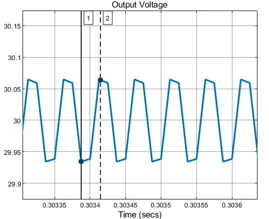
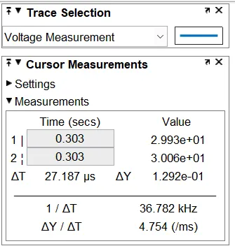
`V_(out_(avg)) = 30V` as expected by the requirement. In the above zoomed out view, it can be seen at 0.5sec when the `V_(i n)` changes from 40 to 50V, the output remains at 30V after a transient overshoot. Hence confirming the working of the closed loop control.
`DeltaV_(out) =`0.01292V which is `lt 0.3V` as calculated.
Output Current
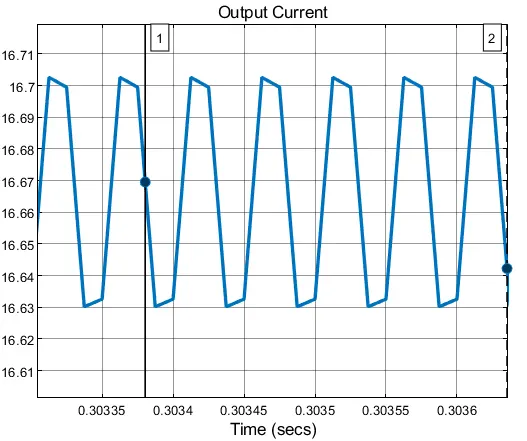
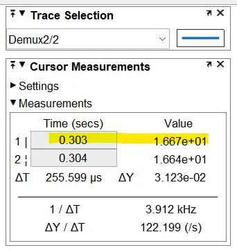
`I_(o_(avg)) = 16.67A` which is same as calculated.
Inductor Current
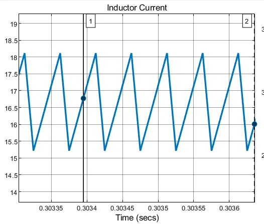
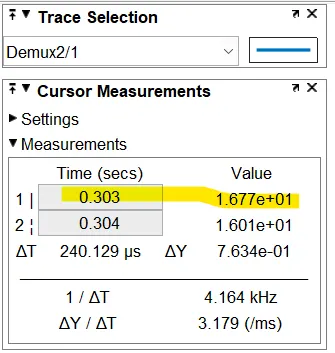
`I_(L_(avg)) = 16.67 A` as calculated`
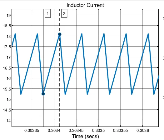
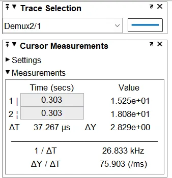
`DeltaI_L = 2.829A lt 5.001A` as calculated
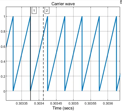
Carrier wave of frequency 20kHz. This is the frequency at which the MOSFET should be turned on & off.
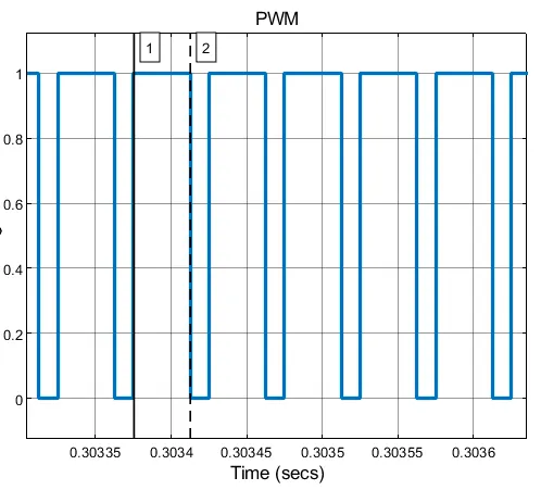
PWM fed to the MOSFET
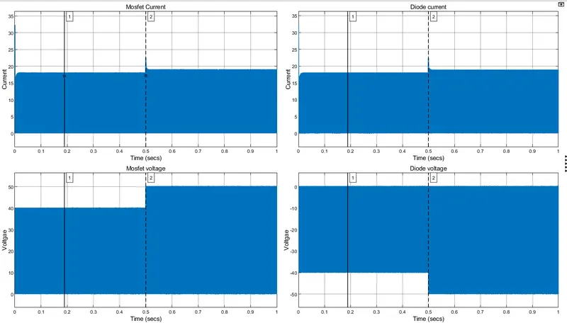
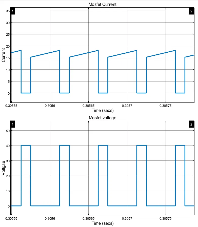
MOSFET current & voltage
Peak current = 18.12A
Peak voltage = 40.22V
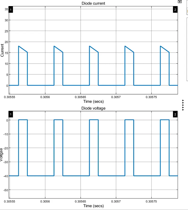
Diode Current & voltage
Peak voltage = -40V
Peak current = 17.94A
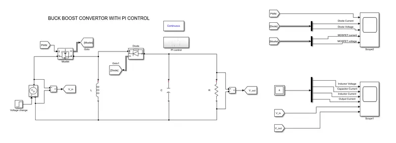
BuckBoostConvertor_withPIcontrol.mdl
Buck boost convertor is a type of DC DC convertors which converts a particular range of DC voltage to stable output DC voltage which could be higher or lower than the input voltage. The buck boost convertor consists of two semiconductors switches(MOSFET & diode), one inductor & one capacitor. The input source is directly connected to the MOSFET. The MOSFET is turned ON & OFF by PWM signals. When MOSFET is turned ON, the inductor is charged. At this time, the diode is reverse biased & hence doesn't conduct. When MOSFET is turned OFF, inductor discharges through diode & capacitor & this cycle continues.
The main disadvantage with buck boost convertor is the output voltage is -ve which makes the convertor designing difficult. Also, the voltage stress across the active components is very high. Due to non avaliablity of inductors in input & outpust side, for running the convertor in CCM, very large capacitors are required.
Following are the assumptions made in regards with the schematics:
`DeltaI_L = 30% of I_o`
`f_s = 20kHz`
`DeltaV_(out) = 1% of V_(out)`
Following are the calculations which are done to obtain the component values:
`R = V_(out)^2/P_(out)` = 6.75`Omega`
`I_o = P_(out)/V_(out)` = -6.67A
`I_(L_(avg)) = I_o/(1-D)` = 16.67A`
`V_(out)/V_(i n) = -D/(1-D)`
For `V_(i n) = 30V` , D = 0.6`
For `V_(i n) = 60V`, D = 0.429`
`DeltaI_L =` 2A
`DeltaV_(out) =`0.45V
`L = (V_(out)(1-D))/(f_sDeltaI_L)` = 450 `muH`
`C_(out) = D/(Rf_s((DeltaV_(out))/V_(out))` = 444.44`muF` for D =0.6
ZOOMED OUT VIEW
ZOOMED IN VIEW
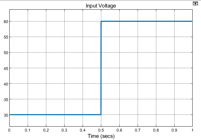
Input Voltage
`30VleV_(i n)le60V`
Output Voltage
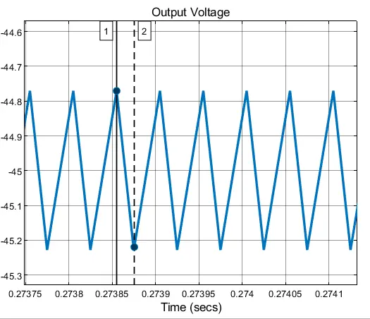
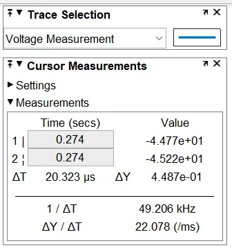
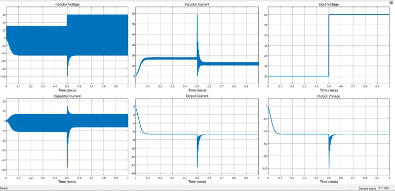
`V_(out_(avg)) = -45V` as expected by the requirement. In the above zoomed out view, it can be seen at 0.5sec when the `V_(i n)` changes from 30 to 60V, the output remains at -45V after a transient overshoot. Hence confirming the working of the closed loop control.
`DeltaV_(out) =0.4487V`which is `lt 0.45V` as calculated.
Output Current
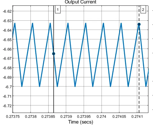
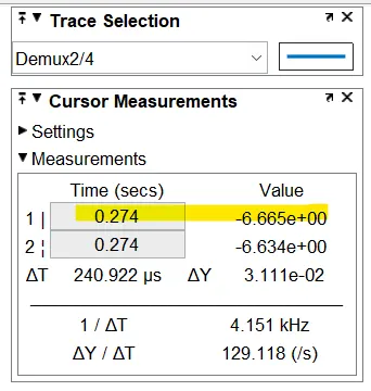
`I_(o_(avg)) = -6.665A``~~-6.67A`
Inductor current
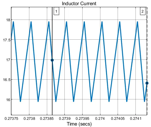
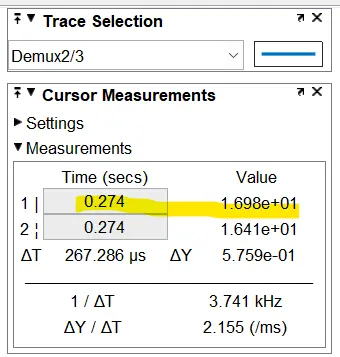
`I_(L_(avg)) = 16.98A``~~16.67A`
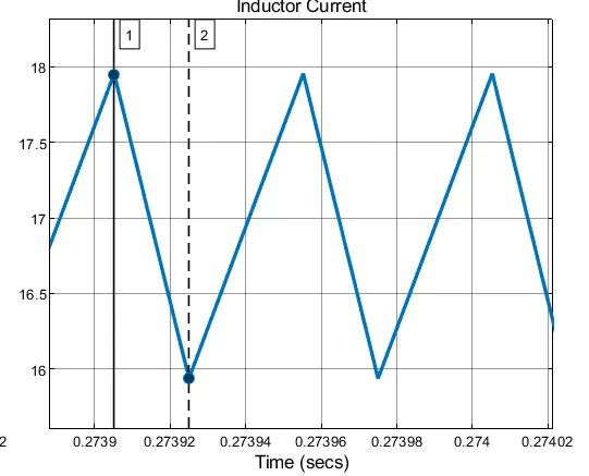
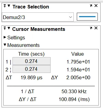
`DeltaI_L = 2A` which is equal to 2A as calculated above.
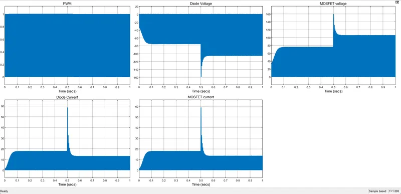
Carrier wave of frequency 20kHz
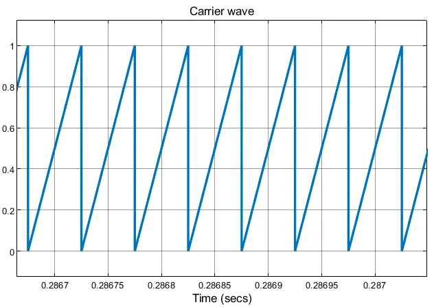
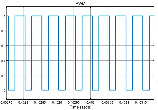
PWM fed to the MOSFET
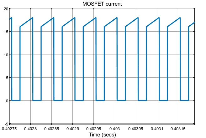
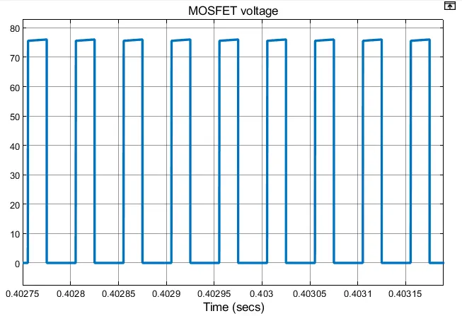
MOSFET current & voltage
Peak Current = 17.92A
Peak Voltage = 75.76V
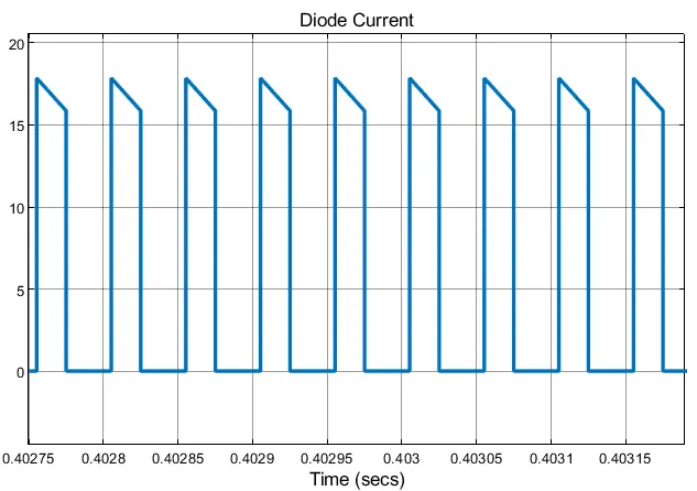
Diode Current & Voltage
Peak Current = 17.65A
Peak Voltage = -74.86V
BoostConvertor_withPIcontrol.mdl
In IC, sometimes it is required to have a higher voltage at output when we may have a lower voltage supply. One of the switched mode DC DC convertors called the boost convertors or the step up convertors is used.In other words, its like a step up transformer i.e it steps up the level of DC voltage (while transformer step up / down the level of AC voltage) from low to high while decreases the current from high to low while the supplied power is same. The frequency used is 60kHz which will be possible using a MOSFET as it has lower switching losses as compared to BJT. The inductor is connected next to input signal which boosts the power fed to the output whenever the MOSFET is on. This is the basic idea of the boost convertor. When the MOSFET is on, the inductor & capacitor gets charged. The inductor & capacitor are designed based on the amount of ripple allowed in the output voltage & Output current. When the MOSFET is off, the inductor discharges through the diode & the capacitor discharges through the resistance. The inductor helps in reducing the ripple of the output current & the capacitor helps in reducing the ripple of the output voltage.
Following are the assumptions made in regards with the schematics:
`DeltaI_L = 30% of I_o`
`f_s = 60kHz`
`DeltaV_(out) = 1% of V_(out)`
Following are the calculations which are done to obtain the component values:
`R = V_(out)^2/P_(out)` = 6.75`Omega`
`I_o = P_(out)/V_(out) = 10A`
`I_(L_(avg)) = I_o/(1-D) = 20A`
`V_(out)/V_(i n) = 1/(1-D)`
For `V_(i n) = 200V , D = 0.5`
`V_(i n) = 300V, D = 0.25`
`DeltaI_L =` 3A
`DeltaV_(out) =`4V
`L = (V_(i n)D)/(f_sDeltaI_L)` = 0.55mH for D = 0.5
`C_(out) = D/(Rf_s((DeltaV_(out))/V_(out))` = 0.0208mF for D =0.5
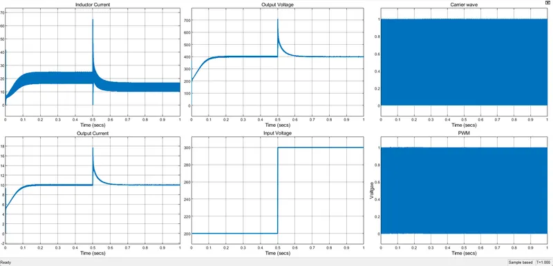
ZOOMED OUT VIEW
ZOOMED IN VIEW
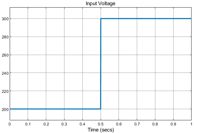
Input Voltage
`200leV_(i n)le300V`
Output Voltage
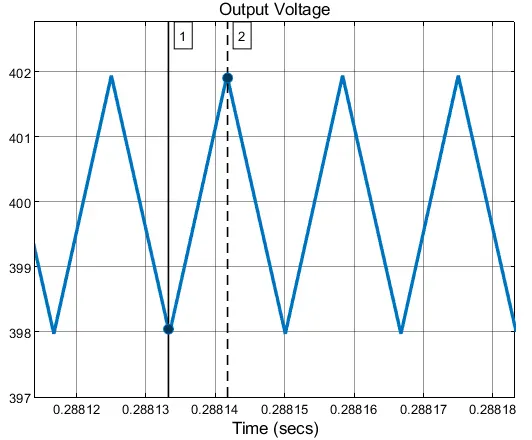
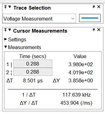
`V_(out_(avg)) = -400V` as expected by the requirement. In the above zoomed out view, it can be seen at 0.5sec when the `V_(i n)` changes from 200V to 300V, the output remains at 400V after a transient overshoot. Hence confirming the working of the closed loop control.
`DeltaV_(out) =3.858V`which is `lt 4V` as calculated.
Output Current
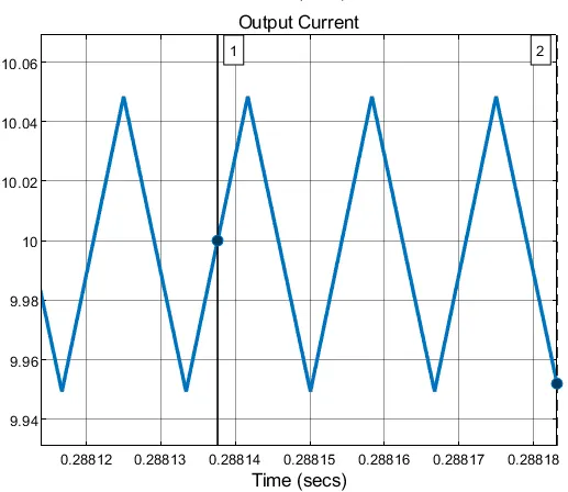
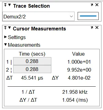
`I_(L_(avg)) = 10A` which is as calculated
Inductor current
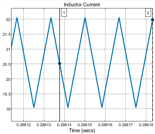
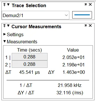
`I_(L_(avg)) = 20.52A` `~~ 20A`
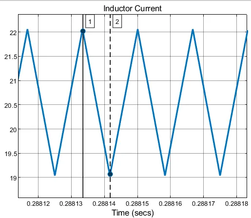
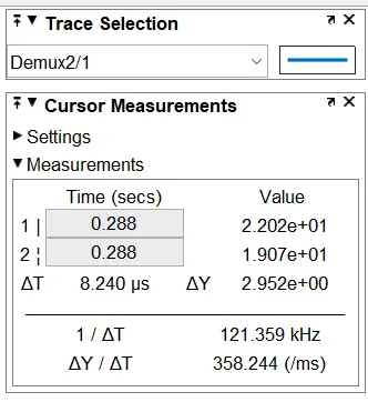
`DeltaI_L = 2.952A lt 3A`which is calculated.
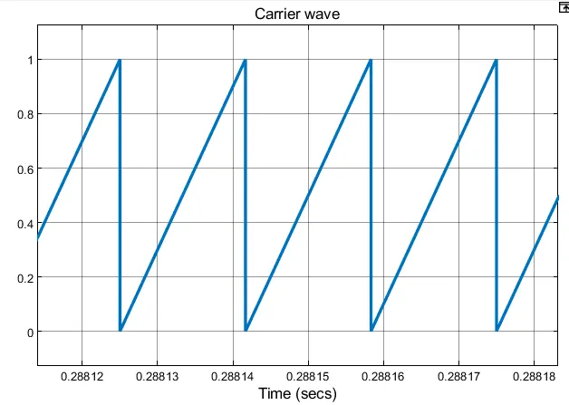
Carrier wave of freq 60kHz
PWM fed to MOSFET
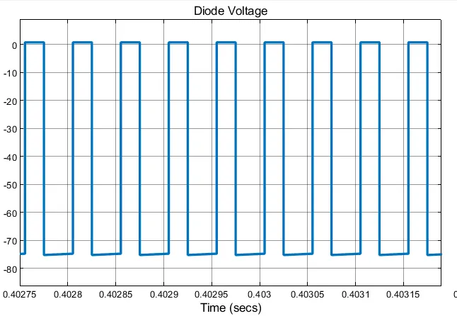
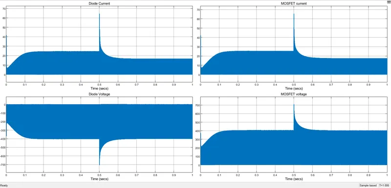
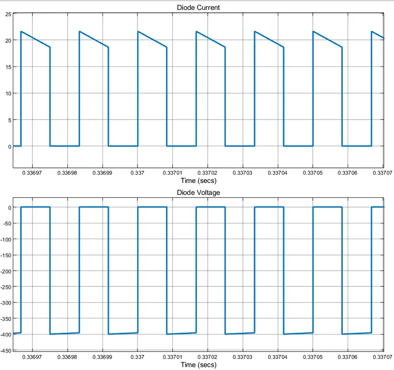
Diode Current & Voltage
Peak current = 21.57A
Peak voltage = -399.4V
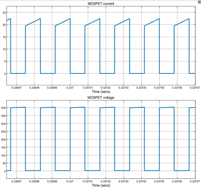
MOSFET current & voltage
Peak current = 22.39A
Peak Voltage = 399.3V