Project 1 - Loss calculation for a DC/DC converter-MATLAB
Design of boost converter, and calculating the loss of different components including power switching device and deriving efficiency of boost converter. This is applicable in power supply industry, electric vehicles etc where DC-DC converter is required to boost the voltage from DC source. All the aspects of this project with loss calculation, device selection, simulation etc are industry relevant.
Aim) The main aim is to Design the Simulink model of the BOOST converter and determine the Losses of the Converter and the efficiency of the Converter.
Answer)
BOOST CONVERTER:-
A boost converter (step-up converter) is a DC-DC power converter that steps up voltage (while stepping down current) from its input (supply) to its output (load).
It is a class of Switched mode power supply (SMPS) containing at least two semiconductors (a diode and a Transisiter) and at least one energy storage element: a capacitor, inductor, or the two in combination.
To reduce voltage ripple ,filters made of capacitors (sometimes in combination with inductors) are normally added to such a converter's output (load-side filter) and input (supply-side filter).

Boost converter schematic
Simulink Model :-
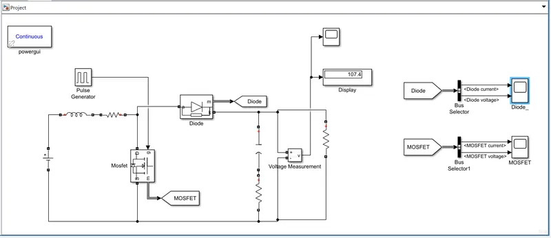
for designing the Boost converter in Simulink we are used the following blocks:
- DC Voltage source
- MOSFET
- Diode
- series RLC branch
- Voltage measurement block
- PWM generator
- Display
- Bus selector
- Power gui
- Scope
Design parameters :-
- Vin = 100 V
- Vout = 200 V
- L = 200uH
- C = 400uF
- R= 10 Ohms
- rL = 10 mOhms
- rC = 2 mOhms
- rd=5 mOhms
- switching frequency=
For duty cycle:-
We know that the
Vo / Vin =(1/ (1-D) )
were,
vin= Input voltage
Vo= Output Voltage
D= Duty cycle
from the given data
Vin = 100 V
Vout = 195.5 V
Then from the above equation
Vo / Vin =(1/ (1-D) )
200/100 = (1/ (1-D) )
2*(1-D)= 1
(1-D) = 0.5
D=0.5
therefore
Duty cycle = 0.5
Simulink Model:-
The Simulink model of the Boost converter will be as follows:-
Procedure:-
For creating the Simulink model of the BOOSt converter The supply voltage and Series RL branch will be connected in a series manner
And MOSFET" acts as a power switch and it is connected in the Parallel manner
After that, a Capacitor and load(Resistive Load) are connected parallel with using the "Series RLC branch" block.
For on and of Switch we are sending the Pulses with switching frequency ()Using a DC-DC PWM generator Block. we are assigning the Duty cycle ratio as 0.5 by using the Constant block.
And the output voltage will be displayed by using the display block.
The voltage and currents drwan by both "MOSFET " and Diode" will be plotted by using the Scope and Bus selector Blocks.
Design Parameters Values:-
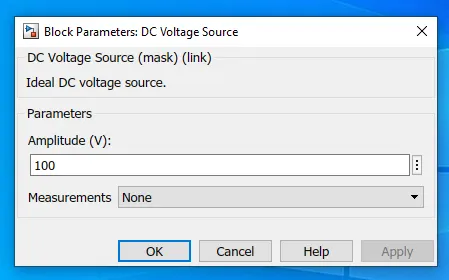
Dc voltage soure :-
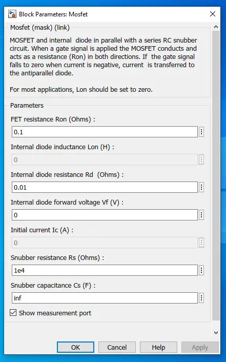
MOSFET parameters :-
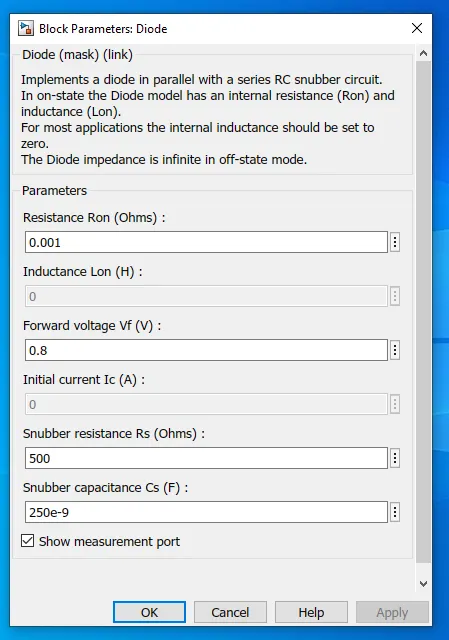
Diode Parameters:-
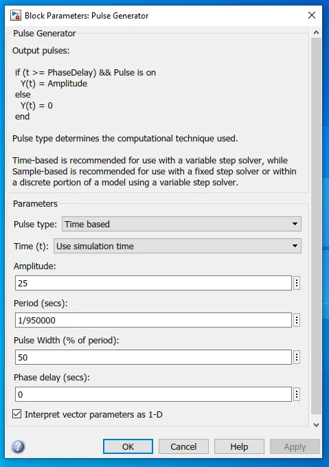
Pulse generator parameter Block:-
OUTPUT SCOPES:-
Output voltage:-
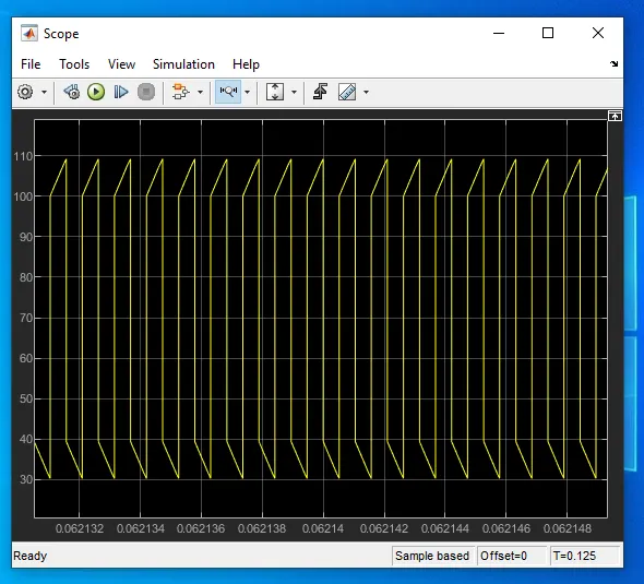
From the above graph, we can see the Output voltage is greater than the Input voltage
Hence the Working of Boost Converter is working in a proper manner
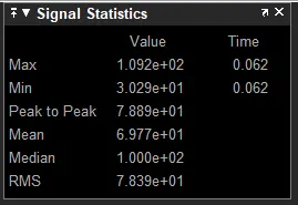
the minimum and maximum Voltage will be displayed by using the Below Signal statistics block.
The Minimum Voltage is 3.029 V
The Maximum voltage is 109.2 V
MOSFET VOLTAGE AND CURRENT:-
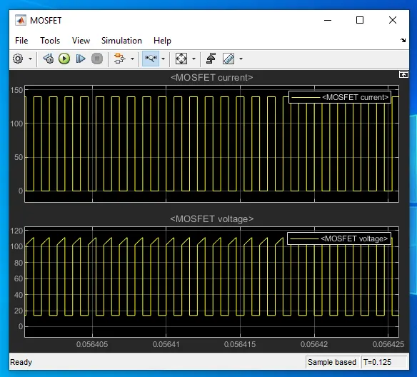
From the above graph, the top graph will be the Mosfet Current Graph
Bottom Graph will be the Voltage graph
we can observe that the 0.5 Duty cycle ratio in the graph
The Minimum And maximum Currents in MOSFET will be determined by using Signal statistics Below
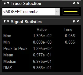
Maximum Current =139.5 Amps
Minimum current = 0.0Amps
Voltage in MOsfet will be understand by using below Signal statistics
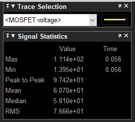
The minimum Voltage in MOSFET = 13.95 V
the maximm voltage in MOSFET= 111.4 V
DIODE VOLTAGE AND CURRENT:-
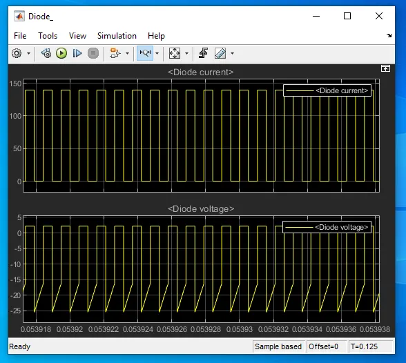
From the above graph the top graph will be the DIODE Current Graph
Bottom Graph will be the Voltage graph
we can observe that the 0.5 Duty cycle ration in the graph
The Minimum And maximum Currents in Diode will be determined by using Signal statistics Below
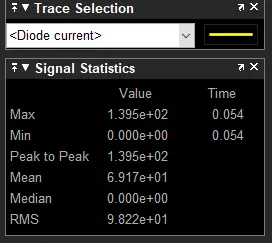
Maximum Current =139.5 Amps
Minimum current = 0 Amps
Voltage in Diode will be understand by using below Signal statistics
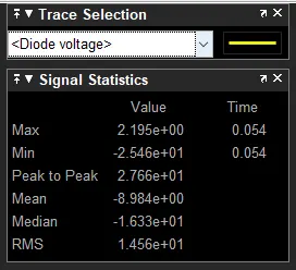
The minimum Voltage in Diode = -2.546 V
the maximm voltage in Diode=2.195 V
Determining the Losses in Powe Electronic Converters:-
In any DC-DC converter majorly consider 4 types of losses as followes:-
- Conduction Losses
- Diode losses
- Induction Losses
- Capacitor Losses
Conduction Losses:-
Conduction losses are a result of device parasitic resistances impeding the DC current flow in a DC/DC converter. These losses are in direct relationship with the duty cycle.
When the integrated high-side MOSFET turns on, the load current flows through it. The drain-to-source channel resistance (RDSON) causes power dissipation.
Formula:-
Conduction Losses:- Pc= I² * R *D-----------------(1)
were,
p= Power Dissipation
I= Current through MOSFET
R= Resistance in Ohm
D=Duty Cycle= Vout / Vin
Diode losses:-
The diode is forward-biased when the integrated MOSFET turns off. During this time, the inductor current ramps down through the output capacitors, the load, and the forward-biased diode. Since the load current is now conducting through the diode, there will be power dissipation in Diode.
This will be calculated by using below Formula:-
Diode Losses:- P= Vf * I* (1-D) ------(2)
were,
Vf= forward voltage
I= Current output
D=Duty Cycle= Vout / Vin
Induction Losses:-
The conduction losses depend on the load current. With heavier loads, the conduction loss in the MOSFET increases and is the dominating factor. Conduction losses plus switching, driver and internal low-dropout regulator (LDO) losses lead to a considerable generation of heat.
This losses can be calculated by using the below formula:
Pd= I² * R + { (rl / 12) (D* Vin / F*L)}-------(3)
were,
I= Current output
D=Duty Cycle= Vout / Vi
F= Frequency
L= Inductance value
Capacitance losses:-
While getting the output through the capacitor we can get some power dissipation in the capacitor also.
this power dissipation is determined by using the following Formula:-
Pc= {rc* D*(1-D) I² + {rc / 12(1-D)}}*{(Din / C*F)}----(4)
were,
I= Current output
D=Duty Cycle= Vout / Vi
F= Frequency
C= Capacitance value
From the given data we can find the losses for the Designed DC-DC Converter:-
Vin = 100 V
Vout = 200 V
L = 200uH
C = 400uF
R= 10 Ohms
rL = 10 mOhms
rC = 2 mOhms
rd=5 mOhms
Duty cyclee= 0.5
Conduction Losses:-
from equation (1)
Conduction Losses:- Pc= I² * R *D
Pc= (1)² * 10*0.5
Conduction Losses (Pc)=5W
Diode losses:-
From equation (2)
Diode Losses:- Pd= Vf * I* (1-D)
= 19.55 * 1 * (1-0.5)
= 19.55*0.5
Diode Losses(Pd) =9.75 w
Inductior Losses:-
From the equatation (3)
PI= I² * R + { (rl / 12) (D* Vin / F*L)}
=1² * 10 +(0.0008*5000)
= 10+4
PI =14 W
Capacitance Losses:-
From the equatation (4)
Pc= {rc* D*(1-D) I² + {rc / 12(1-D)}}*{(Din / C*F)}
=2*0.5*0.5+(2*0.0001*0.5*0.5*100 / 400*50*0.000001)
Pc= 0.7085 W
Total Losses= Pcon+Pd+Pi+Pc
=5+9.775+1.4+0.7085
Total losses=11.74585 W
Efficiency Of Converter:-
The Efficiency Of the converter is determined by using below formula:
Formula:-
Efficiency = (Pin -Ploss / Pin ) 100-----------(5)
From the data
Pin= Vin * I
I= Vin / R
=100 / 10
I= 10 Amps
Therefore,
Pin = vin * I
=100 * 10
Pin=1000 W
From above equation(5)
Efficiency = (Pin -Ploss / Pin )100
= 1000-11.75 / 1000 100
Efficiency = 98.825 %
Results:-
The total Power losses Ploss= 11.75 W
The efficiency of Converter = 98.825 %
CONCLUSION
The outcomes for the project given are met as per the requirements