Project 1
Solution:
In the above CCM(40 to 50 and 400 to 500V),Boost CCM(20to-30V and 200 to-300V) and sepic (30-60V and 300 to-600V) are chosen.
Totally 6 topologies are chosen.
Buck converter:
Buck converter in contious mode:
Buck converter does DC-DC conversion.
Buck converter step down DC voltage. It consists of inductor, capacitor and two switches which are tranistor and diode. Transistor (moseft or igbt based on application ) is a switch that operates with on and off state.ON and OFF states get controlled by the Gate signal.
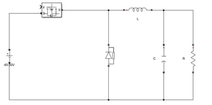
This is the buck converter used to convert DC to DC with step down operation.
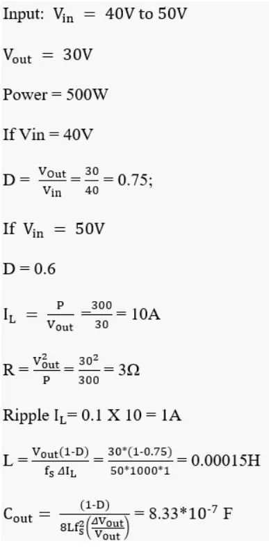
Vin L C
40 0.00015H 8.33*F
50 0.00024H 8.33*F
The simulation circuit shows the buck converter.
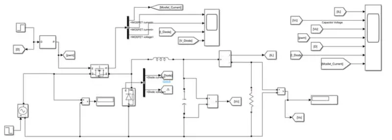
The result of simulation are as below.
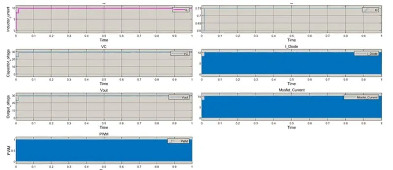
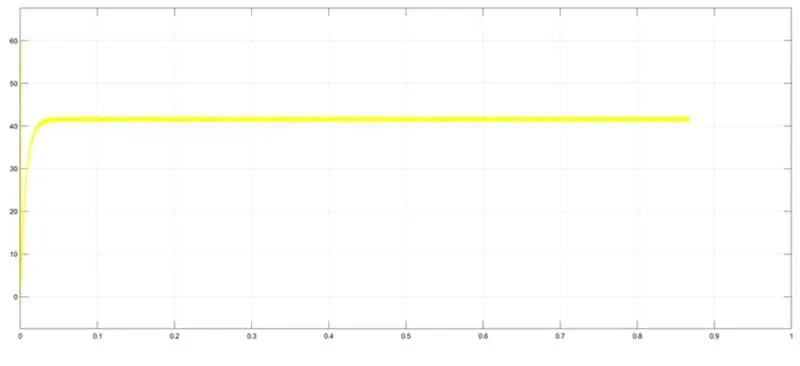
It shows that the output voltage 30V and the capacitor voltage is the same as output voltage.
The inductor current has resulted as 10A.
ON and OFF operation of a switch is with the frequency 50khz and shown in below.
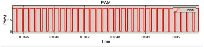
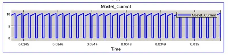
The Diode current and Mosfet current is shown below.
If the same buck converter parameters are modified as the
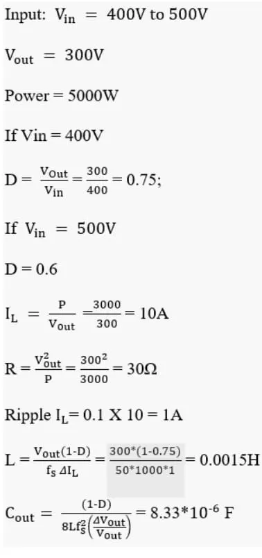
Vin = 400 to 500V
Output voltage = 300V
Power = 3KW
Below are the rating requirements for the inductor, capacitor and resistor.
Vin L C
40 0.00015H 8.33*F
50 0.00024H 8.33*F
Matlab circuit simulation as shown below:
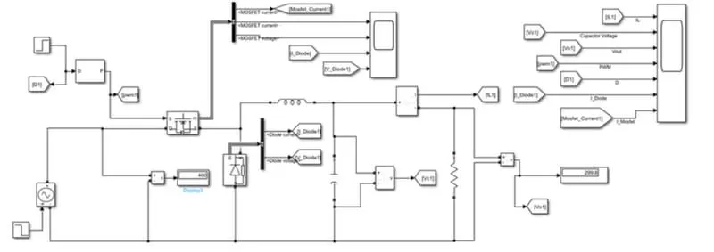
below are the responses of PWM current in diode and MOSFET current.
Below are the waveform which tells that the MOSFET in ON and OFF with the PWM signals.Diode is on for a period of time MOSFET is ON in other period which is shown in the below graphs.
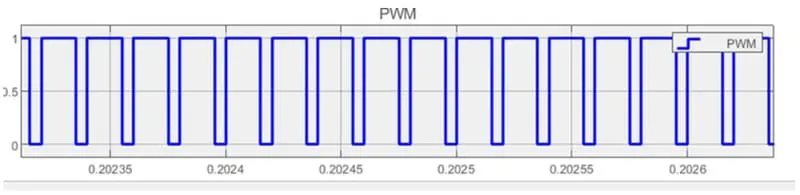
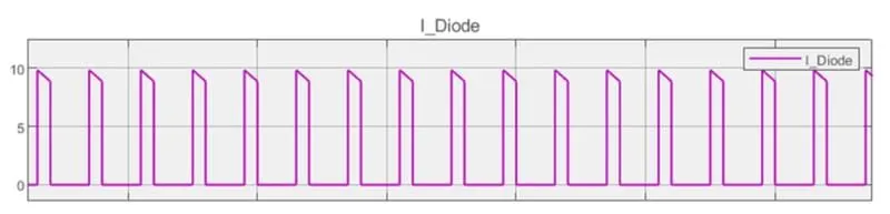
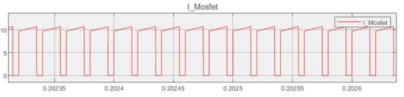
Inductor and capacitor values are taken in such a way that the L and C values are high. As the input voltages range is from 40 to 50 and 400 to 500 in another buck converter.
As per the different input values, the inductor and capacitor values are designed accordingly.
Boost_converter CCM:
Boost Converter:
The boost conveter is the step up DC-DC converter. The output capacitor is the one that filters the plusating current and allows DC current to flow through the output.
In continuous conduction mode. the inductor current flows continously during the operation of the converter.The two semiconductors during the operarion of the converter. The two semi conductors switches in opertion are diode and Mosfet which operate with the PWM pulses. MOSFET is a switch whose gate pulses are given by the PWM pulse generator based on the duty required to the switch.
It is considered that the frequency is considered as 30KHZ.
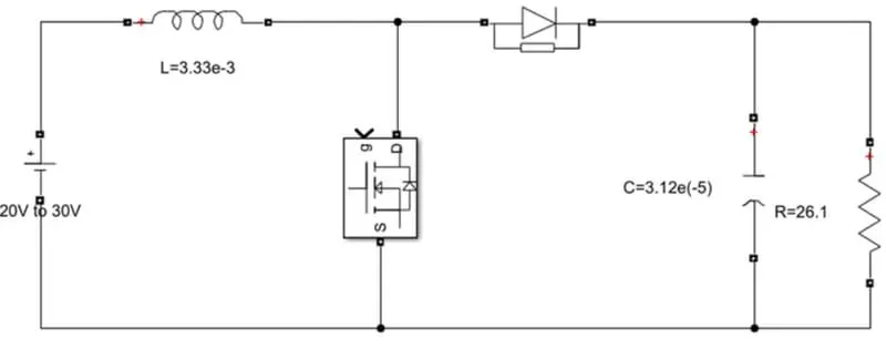
The schematic of boost converter is an showns below.
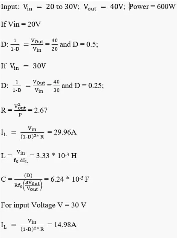
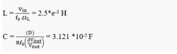
The mathematical expression and calculations in desiging the required inductor and capacitor values.
Simulink file of Boost converter.
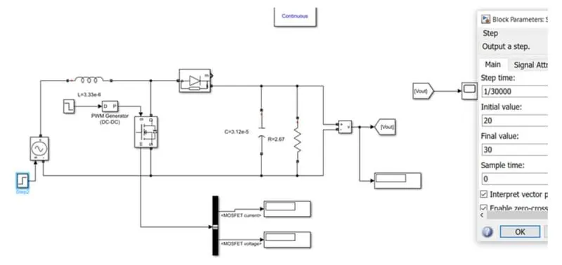
After the simulation is compiled,the simulation file is an shown below.
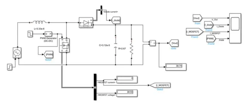
Simulation displays that the output voltage after the run simulation shows that the output voltage is reaching 40V.
Other results are shown below.
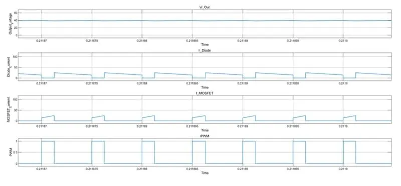
The zoomed results of the Boost converter are shown in the above results.
it shows the output voltage is 40V diode current and MOSFET current are showing that the switches are operating alternatively and PWM signal is swiching on the MOSFET into ON and Mosfet is OFF when PWM signal is OFF.
The above boost converter results if the input voltages are modified the results vary as shown below.
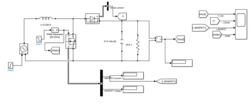
Matlab simulation file:
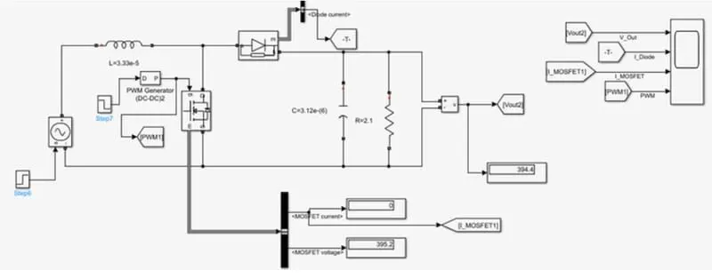
Boost converter displays is as shows below:
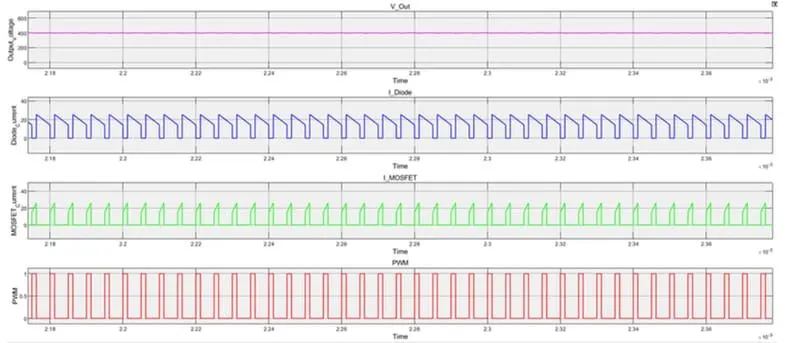
Diode, Mosfet current and PWM signals are shown below for the input voltage of 200V to 300V.
output voltage is expected as 400V and the diode and current operates with different ON and OFF situations.
Diode current is ranging upto 20A and MOSFET current is ranging upto 25A. where the PWM pulses shown the ON and OFF states of the MOSFET.
5.sepic converter:
SEPIC converter:
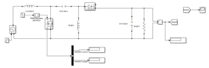
sepic converter is the single ended primary inductor converter. This is a type of DC-DC converter that operates to allow the electrical output greater than, less than, or equal to the input output is controlled by the duty cycle of the switch.
sepic converter is a boost converter followed by inverter Buck-Boost converter.
Vin is 30V to 60V:
Vout is 45V
power P =1
D/(1-D)=Vout/Vin
so D=0.6
As there are two inductors in the circuit the inductor_1L1 is at the voltage input of the circuit and onother inverter is at the parallel end.
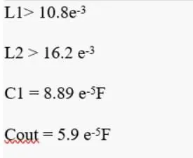
From the calculation as per the instructor the values of L and C are designed as
Below are the output waveforms of the circuit
Output voltage is varying between 41 to 42V