Project 1 - 40-V to 80-V adjustable output voltage boost reference design for LIDAR applications
Q
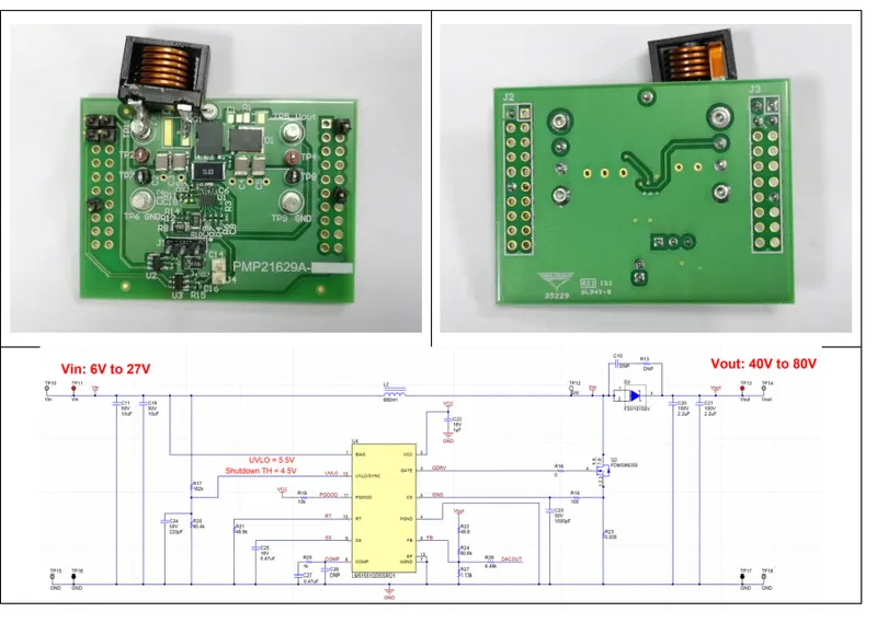
This reference design utilizes a non-synchronous boost controller to provide an adjustable output of between 40 V
and 80 V capable of delivering a maximum of 100 mA of current to the load. This is an Automotive design
intended to power various applications such as LiDAR systems, which require an adjustable voltage supply.
Ans:-
1 Test Prerequisites
1.1 Voltage and Current Requirements
| PARAMETER | SPECIFICATIONS |
| V(in) | 6-27VDC |
| V (out) | 40VDC to 80VDC (adjustable) |
| I (out) | 0.1A Maximum |
| F(ws) | 400kHz Nominal |
1.2 Required Equipment
Power Supply
Load Resistors
DMMs
Oscilloscope
Auxiliary Power Supply (for providing DC signal that controls the output voltage)
1.3 Considerations
Using electronic loads may exhibit undesirable behavior due to the interaction of the regulation loop of the
electronic load with the low output capacitance of the boost converter. It is recommended to use resistor loads
instead.
2 Testing and Results
2.1 Efficiency Graphs
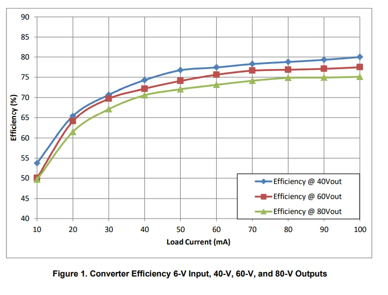
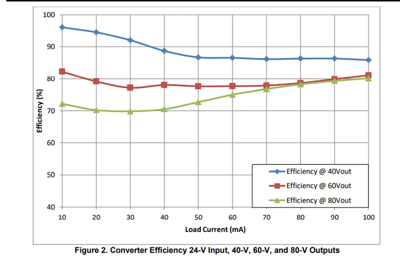
Figure 1 shows the converter efficiency for an 18-V input with 35-V, 100-V, and 150-V outputs.
2.2 Efficiency Data
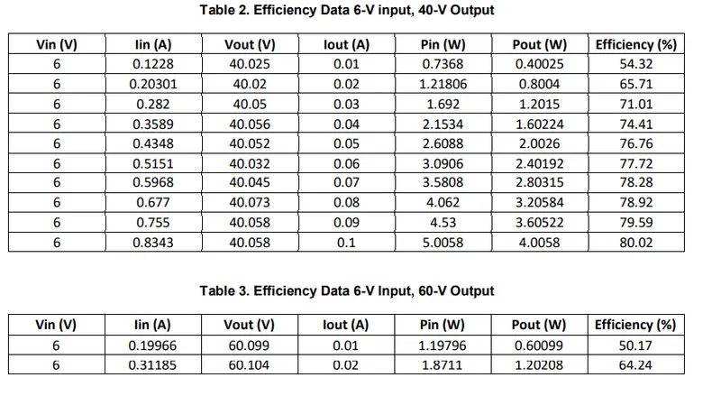
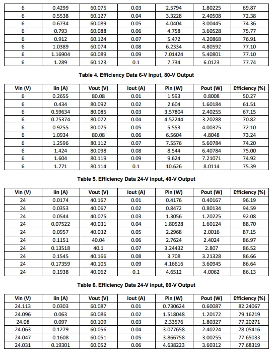
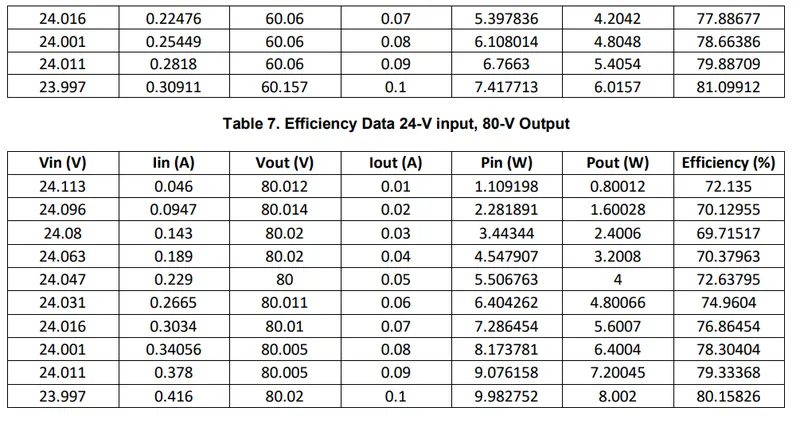
Table 2, Table 3, and Table 4 show the efficiency data for 40-V, 60-V, and 80-V outputs with 6-V input. Table 5,
Table 6, and Table 7 show the efficiency data for 40-V, 60-V, and 80-V outputs with a 24-V input.
1. How will you decide the layer stack up
Multilayer PCBs are the result of the demands of miniaturization, lightweight, multiple functionalities, and high speed for modern electronics. A multilayer PCB contains at least three or more conductive layers. Interference, noise, and stray capacitance may exist if the layer arrangement is inefficient when it comes to complex and high-density PCBs. An optimal multilayer stack-up benefits the end product greatly.
l Poor stacking will cause EMI (electromagnetic interference) radiation to rise because reflections and ringing in the system can significantly reduce product performance and reliability due to impedance mismatches.
l Layer stack-up allows getting more circuits on a single board through the multilayer design of PCBs.
l A well-designed layer stack-up can increase the EMC of a product.
l An excellent layer stack-up can both minimize radiation and prevent the circuit from interference from external noise sources.
l Carefully stacked PCB substrates can also reduce signal interference and impedance mismatch issues.
l Good PCB layer stack-up helps to balance the demands for cost-effective manufacturing methods with concerns about signal integrity issues.
Some tips in PCB layer stack-up
No matter how many layers a PCB design has, the specifications of trace widths, pad spacing, copper weight, and drill sizes must be in line with the PCB manufacturing capacity. And for PCB fabrication and assembly, the number of layers, the arrangement or stack-up of layers, and the material types are significant effects. There are several tips for a better design of layer stack-up:
1. Determine the number of the layers
The primary consideration for PCB stack-up is determining how many layers are needed. This includes the signal type (high speed or low speed), power (a part of the circuit or for high power boards), ground layers, or planes. Do not mix the signal types on the inner layers.
2. Determine the layer arrangement
The number of layers can be predicted according to the pin density. And how to arrange the layers should follow some rules. Firstly, place the signal layer next to the internal power plane for tight coupling. Secondly, the space between the power layer and the ground layer should be minimal. Thirdly, avoid having two signal layers next to each other. Fourthly, make the stack symmetrical inward from the top and the bottom layers.
3. Determine routing and vias
The routing of the traces, the copper weight, the position of vias, and the vias' type of implement, are the essential factors of layer stack-up.
4. Determine the material types of the layers
There are standard thickness and other properties for various circuit board materials. Therefore, the thickness of each signal layer and the thickness of the prepreg and cores need to be determined according to the electrical, mechanical, and thermal properties of different board materials.
NextPCB provides multilayer PCBs with layers from 4 to 16 layers, board thickness from 0.6 to 2.5mm, outer copper weight from 1 to 3 oz, and inner copper weight from 0.5 to 1 oz. If you need more information about the default stack-up of standard PCB, custom PCB stack-up service, or layer stack-up for PCB prototype, please contact online services, you will get answers very quickly.
2. How do you calculate the trace width, via size and trace length?
Trace width is an important design parameter in PCB design. Adequate trace width is necessary to ensure the desired amount of current can be transported without overheating and damaging your board. You may use this online tool to calculate an estimate of the minimum trace width for a given current and copper weight. A higher current requires thicker traces while a thicker copper weight allows for thinner traces.
Table of Bittele production minimum sizes
| Copper Weight | 0.5oz | 1oz | 2oz | 3oz | 4oz or above | |
| Outer layers | Minimum Trace Width | 3mil | 4mil | 5mil | 6mil | RFQ |
| Minimum Trace Spacing | 4mil | 5mil | 7mil | 10mil | RFQ | |
| Via holes to other copper feature | 7mil | 9mil | 12mil | 16mil | RFQ | |
| Inner layers | Minimum Trace Width | 3mil | 3.5mil | 5mil | 6mil | RFQ |
| Minimum Trace Spacing | 3mil | 4mil | 6mil | 9mil | RFQ | |
| Via holes to other copper feature | 7mil | 8mil | 11mil | 15mil | RFQ |
Notes:
The formula for calculating allowable current through a trace is published in the IPC-2221 standard section 6.2 as shown below.
Internal traces : I = 0.024 x dT0.44 x A0.725
External traces: I = 0.048 x dT0.44 x A0.725
Where I am maximum current in Amps, k is a constant, it is temperature rise above ambient in °C, & A is a cross-sectional area of trace mils².
The trace width can then be calculated by rearranging this formula to determine the cross-sectional area that our desired current can safely pass through.
Area[mils^2] = (100[Amps]/(k*(Temp_Rise[deg. C])^ 0.44))^(1/0.725)
Then, the Width is calculated from the cross-sectional area for a chosen thickness:
Width[mils] = Area[mils^2]/(Thickness[oz]*1.378[mils/oz])
As per IPC-2221 for internal layers k = 0.024 and for external layers: k = 0.048
Disclaimer:
These calculations are industry standard and believed to be correct, but not guaranteed. May not be appropriate for all designs.
Below is the formula for resistance of a trace:
Resistance = Resistivity*Length/Area*(1 + (Temp_Co*(Temp - 25))
Where, Area = Thickness*Width
A copper Thickness of 1 oz/ft^2 = 0.0035 cm
Copper Resistivity = 1.7E-6 ohm-cm
Copper Temp_Co = 3.9E-3 ohm/ohm/C
Voltage Drop is Current * Resistance
Power Loss is Current^2 * Resistance
- What is the drawback of having 2 layers of PCB?
Ans:-
Limited design flexibility 2-layer PCB is the most common type of PCB, and it is used in a wide variety of applications. If you are looking for a less expensive option, or if time is of the essence, 2-layer PCB may be the right choice for you. hare having more high limitation of value
The disadvantage only becomes significant in very high-frequency circuits. When multilayer boards depend on ground planes being fractions of a millimeter from the transmission line traces. So designs for high-speed memory, FPGA, GPU, and CPU (for example) require significant trace routing and stack-up engineering. A simple two-sided board is not going to work in those cases. If you are working on a design with frequencies above 100MHz, you may need a multi-layer board. Below that you can use a 2-layer.