Project 1
PROJECT NO:1 BUCK CONVERTER IN CCM(Continuous Conduction Mode)
Given:
Input Voltage range:40-50v
Ouput Voltage:30v
Power level:500W
Lets take switching frequency of 20kHz because of using MOSFET as the switching device in this design of BUCK converter.
Load Details:
Load will be selected as per the power level given and also the resistive load is more suitable compare to any other types of load such as motor, electric bell etc. Instead of resistive load even we can go for Lamp load but the power and load requirement sholud be match with the resistive load. The load requirement is as below.
Load Current,`I_(load)`=`(Power)/V_(out)`=`(500)/(30v)`=16.67A.
Load Resistance,`R_(load)=(V_(out))/(I_(load))=(30v)/(16.67A)=1.8Omega.`
Resistive Load of `1.8Omega,20A`
Design of Inductors and Capacitors
If Input Voltage is Higher then lower average current. If the we take higher average inductor current that lead the lower input voltage to discontinuous conduction mode.
Hence we select the slightly higher input voltage than the highest Operating Voltage.
So Lets take to calcualte boundary Input Voltage as 610V.
|
`V_(out)=30v` |
CCM border condition `V_i=55V` | Max `V_i`=50v | Min `V_i`=40v |
|
Duty ratio ,`D=(V_(out))/(V_i)=30/V_i` |
0.5455 | 0.6 | 0.75 |
Designing of Inductor
Inductance of Buck Converter,`L>(1-D)/(2.fs)*R=(1-0.5455)/(2*20k)*1.8=20.455muH`.
So for the circuit we need a inductor of `20.5muH` of 250A. 226A is peak current of the above CCM border condition design so consider 250A as peak current.
Design of Capacitor
Lets take voltage ripple of 10%.
Capacitance,
`C=(1-D)/(8.L.fs^2.dv)=(1-0.)/(8*18xx10^-6*(20xx10^3)^2*0.1)=694.4muC=700muC`
Selection of Capacitor
- `700muC` /60V.
Note: max output voltage is 40V.
DESIGNING OF CLOSED LOOP CONTROLLER
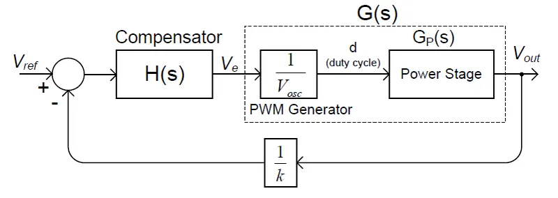
CLOSED LOOP CONTROL FOR BUCK CONVERTER
|
Transfer function for designing of cloosed loop control |
|
|
Power Stage, `G_p`(s) ESR=`0.08Omega` |
`(0.005s+90)/((2.35xx10^-8)s^2+0.118xx10^-3 s+1.8)` |
| Compensator, H(s) | `(149.1xx10^-6 s+1)/((6.993xx10^-10 s^2+4.394xx10^-5 s)` |
| Referrence Voltage, `V_(ref)` | 2v |
| Oscilation Voltage, `V_(osc)` | `(-5v -> 5v)` |
| Voltage reducer(Voltage divider) | `1/k=(V_out*R_(f2))/(R_(f1)+R_(f2))` |
COMPENSATOR SELECTION.
For selection first we need to check these fequency as below
`F_(LC)=1/(2*pi*sqrt(L_oC_o))=1/(2*pi*sqrt(18mu*700mu))=1423.5Hz.`
`F_(ESR)=1/(2*pi*ESR*C_o)=1/(2*pi*0.08*700mu)=2864.79Hz.`
`F_o->(1/10->1/5)`of switching frequency.
Lets take `F_o=1/5 of F_s=1/5of 20xx10^3=4kHz.`
`F_s/2=10kHz.`
|
Compensator Type |
Relative location of the crossover and power-stage frequencies |
|
Type II (PI) |
`F_(LC)<F_(ESR)<F_o<F_s/2` |
|
Type III -A (PID) |
`F_(LC)<F_o<F_(ESR)<F_s/2` |
|
Type III -B (PID) |
`F_(LC)<F_o<F_s/2<F_(ESR)` |
From the above table type II compensator is more suitable for the our buck converter
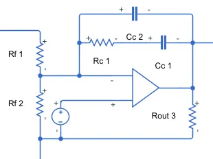
For designing of the above circuit we need do some calculation to find the values of all the elements
`F_(z1)=0.75*F_(LC)=0.75*1423.5=1.0676kHz`
`F_(p0)<F_(LC)`
`F_(p1)=F_s/2=10kHz`.
Lets take `R_(f2)=1kOmega.`
`R_(f1)=(R_(f2)*V_(ref))/(V_(out)-V_(ref))=(1k*2)/(30-2)=14kOmega.`
`R_(C1)=(R_(f1)*F_(ESR)*V_(out)*F_o)/(V_i*F_(LC)^2)=(14k*2864.79*30*4k)/(50*1426.5^2)=475MOmega.`
`C_(C1)=1/(2*pi*R_(C1)*F_(z1))=1/(2*pi*475M*1.0676k)=3.2nF.`
`C_(C2)=1/(pi*R_(C1)*F_s)=1/(pi*475M*10k)=0.33nF.`
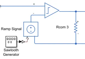
PWM PULSE GENERATOR(Comparator)
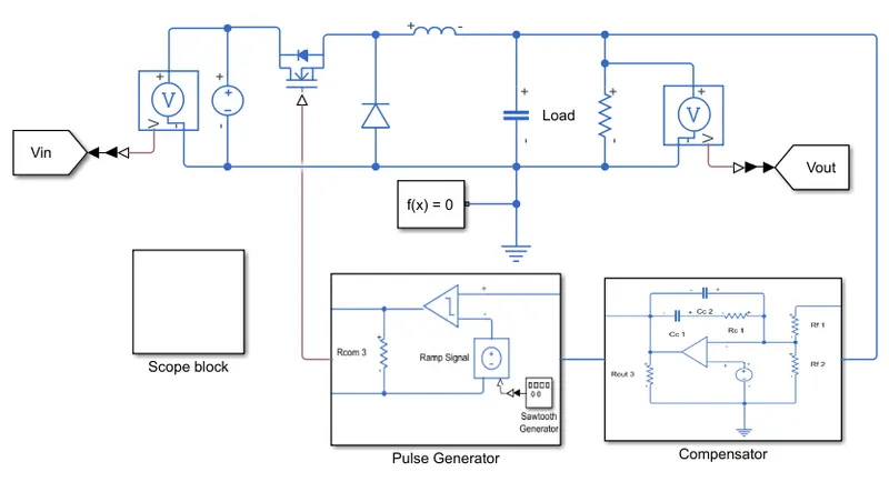
TOTAL SIMULATION
SCOPE OUTPUT AND SIGNALS
| `V_i=40v` | 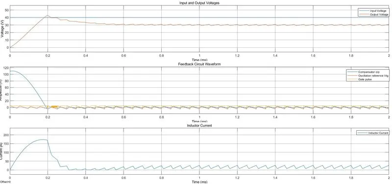 |
|
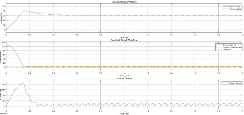
`V_i=50v` |
 |
|
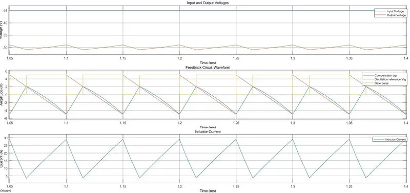
`V_i=45v` zoomed view |
 |
| MOSFET and Diode Voltage and Current | 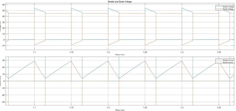 |
RESULT:
| Theoritical | Simulation | |
| `V_i`range | 45V | 45V |
| `V_(out)` | 30V | 29.88V |
| `DeltaV_(out_())` | 10%(28.5-31.5V) | 6.6%(29.06-31.04V) |
| `I_(out)` | 16.67A | 16.57A |
| `I_(L_(avg))` | 16.67A | 16.455A |
| `I_(L_(max))` | 28.8529A | 29.21A |
| `I_(L_(min))` | 4.4871A | 3.693A |
| `DeltaI_L` | 24.3659A(146.17%) | 25.51A(155.03%) |
| `I_(s_(max))` | 28.8529A | 28.819A |
| `I_(d_(max))` | 28.8529A | 28.53A |
All the above result are calculated using the equation mentioned in the buck converter design attached files. And results are compared with the simualtion with help of scope result and all the signal required for observation are given above. Hence forth buck converter is designed along with closed loop feedback circuit includes type II compensator and PWM generator.