Duty cycle
AIM:
- Why power electronics circuits are efficient? In practice, which types of losses occur in power electronics circuits.
- Using a suitable MATLAB model, show how duty cycle control signal can be generated for a simple power converter circuit.
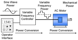
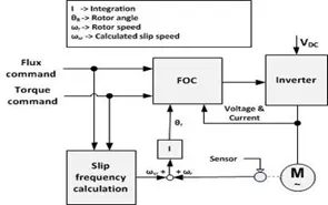
- Explain the difference between VFD and Vector control drive. Can we use VFD method for induction motor in EV applications.
STUDY 1:
Power Electronics is a study of electronic circuit which is used to convert and control the flow of electrical power.It deals with the conversion and control of electric power using semiconductor device such as SCR,IGBT..etc that operates in a switching mode and therefore the efficiency of the devices increases as high as 98-99%.
Power electronic circuits are efficient because
- Power electronic system produces a faster dynamic response compared to electromechanical switch.
- These systems are highly reliable as it is smaller in size compared to mechanical system for similar power rating.
- These devices do not have moving parts so there is less failure of switches so that the performance of switch last long.
- These devices are highly efficient as the power loss is less and switching loss is also minimum.
- There is no maintenance required as there is absence of moving parts.
- The cost of system is low as it is small size,less weight ,less transportation cost.
POWER LOSSES IN POWER ELECTRONICS
The losses are divided into two types:
- Conduction loss
- Switching loss
Conduction loss
Conduction losses occur when the device is in full conduction. The current in the device is whatever is required by the circuit and the voltage at its terminals is the voltage drop due to the device itself. These losses are in direct relationship with the duty cycle.
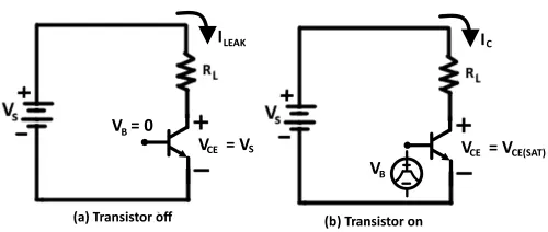
When the transistor is off state :
- The power loss associated with leakage current is
POFF = VS*ILEAK
The leakage current is quite small and does not vary significantly with voltage, it is usually neglected and thus the transistor power loss is essentially zero.
When the transistor is on state :
- When the transistor is on state the small voltage drop across it. This is called Voltage saturation VCE(sat)
- The transistor’s power dissipation or conduction loss due to the saturation voltage is
PON = VCE(sat) *IC
where IC = VS – VCE(sat) / RL
- To control the given application the switch must be turned on and off.Therefore to find voltage power loss duty cycle must be considered.
PON(avg) = VCE(sat)*IC*d
Similarly
POFF(avg) = VS*ILEAK* tOFF/ T
SWITCHING LOSS:
Switching losses occur when the device is transitioning from the blocking state to the conducting state and vice-versa. This interval is characterized by a significant voltage across its terminals and a significant current through it. The energy dissipated in each transition needs to be multiplied by the frequency to obtain the switching losses.
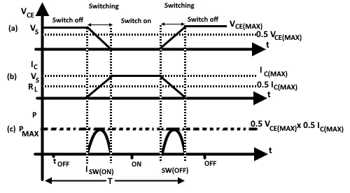
The maximum power loss when switching from off state to on state is
PON(max) = 0.5 VCE(max)*0.5IC(max)
The average value of the waveform is
PON(avg) = 0.637*PON(max)
PON(avg) = 1/6 VCE(max)*Ic(max)
The energy loss during turn on will be PON*tON
WON = 1/6*VCE(max)*ICE(max)*tON
Similarly
WON = 1/6*VCE(max)*ICE(max)*tOFF
The total energy loss in one cycle due to switching is given by
W = WON +WOFF
= 1/6*VCE(max)*ICE(max)*(tON + tOFF)
The average power dissipation in the switch is
PSW = W/T
= W*f
PSW = 1/6*VCE(max)*ICE(max)*(tON + tOFF)*f
The total power loss in switch is
PT = PON(avg) + POFF(avg) + PSW
CONCLUSION:
Thus the power electronics circuits are efficient and the losses are explained clearly.
STUDY 2:
A boost converter (step-up converter) is a dc-dc power converter that steps up voltage (while stepping down current) from its input (supply) to its output (load).
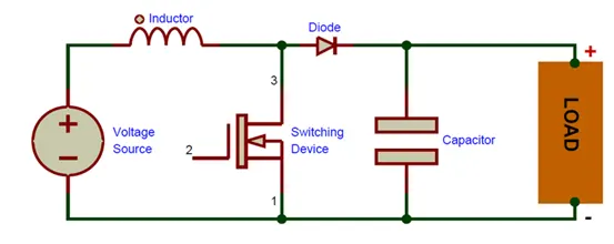
- It is a class of switched mode power supply (SMPS) containing at least two semiconductors (a diode and a transistor) and at least one energy storage element: a capacitor inductor, or the two in combination.
- To reduce voltage ripple, filters made of capacitors (sometimes in combination with inductors) are normally added to such a converter's output (load-side filter) and input (supply-side filter).
MODES OF OPERATION
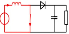
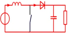
When transistor is ON state :
When the switch is closed, current flows through the inductor in the clockwise direction and the inductor stores some energy by generating a magnetic field as shown below.
When transistor is OFF state:
When the switch is opened, current will be reduced as the impedance is higher. The magnetic field previously created will be destroyed to maintain the current towards the load. Thus the polarity will be reversed (meaning the left side of the inductor will become negative). As a result, two sources will be in series causing a higher voltage to charge the capacitor through the diode D as shown below.
SIMULINK MODEL :
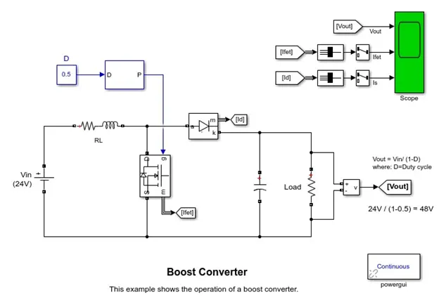
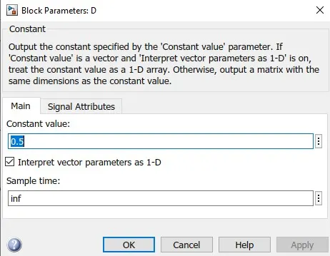
The duty cycle can be varied by using constant block given to PWM pulse is shown below.
OUTPUT:
The duty cycle is 0.5.
The average output voltage of boost converter is
Vo = Vin/(1-D)
where D = duty cycle
Vo = 24/(1-0.5)
= 48V
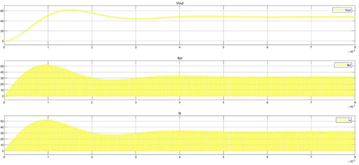
The duty cycle is varied from 0.5 to 0.7.The average output voltage is
Vo = 24/(1-0.7)
= 24/(0.3)
= 80V
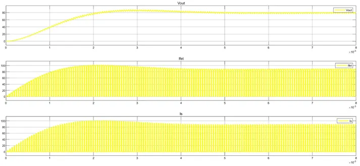
The duty cycle is again varied from 0.7 to 0.8.The average output voltage is
Vo = 24/(1-0.8)
= 24/(0.2)
= 120V
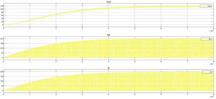
RESULT:
When the duty cycle is varied from 0.5 to 0.8 the average output voltage of buck converter gets increased from 48V to 120V
STUDY 3:
| VARIABLE FREQUENCY DRIVE (VFD) | VECTOR DRIVE |
|
|
|
|
|
|
|
|
 |
 |
EV APPLICATION OF VFD DRIVE
In V/F method flux and current cannot be controlled independently as they are coupled each other in IM.The torque cannot be controlled independently without changing flux value.This makes VFD drive prevent from achieving high efficiency.The stator loss compensation comes into play so precise control is needed which cannot be achieved.Thus the VFD drive is not suitable for EV application.
RESULT:
Thus the comparison of VFD and Vector drive are explained clearly.