Project 2 - SiC/IGBT isolated gate driver reference design with thermal diode and sensing FET
Question:
Description: To design an IGBT or SiC isolated gate driver power stage driving a IGBT module with advanced protection features. The design consists of a single phase power stage from a traction inverter supporting high level of safety features. The IGBT module has integrated thermal diode for temperature monitoring and sensing FET for over current protection, providing fast and accurate protections. It includes the bias supplies and its output voltage monitoring, isolated DC bus sensing in redundant circuits, temp sensing for high side and low side drivers, PWM gate signal monitoring, fault signal injection diagnostics. The supply accepts a wide input range of 4.5V to 65V DC, and delivers up to 180mA output current. The isolated gate driver has up to ±10A drive strength and also includes an analog to PWM converter, which is utilized for temperature and voltage sensing.
Question:
- How will you decide the layer stack up.
- How do you calculate the trace width, via size and trace length.
- What all you do to avoid heating of component in a 4 layer PCB.
- Advantage of multilayer PCB?
Answer:
1) A stackup is the arrangement of layers of copper and insulators that make up a PCB before designing the final layout of the board. Stack-up refers to the arrangement of copper layers and insulating layers that make up a PCB prior to board layout design. While a layer stack-up allows you to get more circuitry on a single board through the various PCB board layers, the structure of PCB stack-up design confers many other advantages. For such a designe a 4 or 6 stack layer will be chosen for the simplicity of the circuit and because the output delivered current is not of hight but ±10A drive strength for the gates of the IGBT .
2)
The important factors to consider when selecting a trace width include:
- The current capacity of the trace
- Space availability and manufacturing limitations
- Trace termination
- Impedance
Then, the Width is calculated: Width[mils] = Area[mils²] / ( Thickness[oz] * 1.378[mils/oz] ). how ever there are the Trance width could be calculated automaticaliy online after giving important parameters such as current, temperature, trace length. For this example we will assume the 6 layer stackup PCB with a thicknes of 1.6mm.
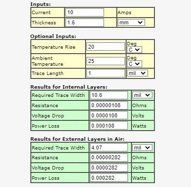
Absolute via sizes are not really specified according to industry standards. Instead, only the minimum sizes are specified based on the size of the component that will be mounted on the via. These standards must be followed if your PCB is to be compliant. The IPC-2222 standard specifies minimum hole diameters for plated through-hole vias for different classes of vias as follows:
- Minimum hole size = Maximum lead diameter + 0.25 mm (Level)
- Minimum hole size = Maximum lead diameter + 0.20 mm (Level B)
- Minimum hole size = Maximum lead diameter + 0.15 mm (Level C)
In addition to standard via sizes, there are also standardized pad sizes that should be used in compliant PCBs. The IPC-2221A standard defines minimum pad sizes for vias as a + 2b + c, where a is the maximum hole diameter, minimum annular ring size, and c is the fabrication tolerance. The fabrication tolerance depends on whether the vias are mechanically drilled or laser drilled, as well as individual process and machining parameters.
The maximum fabrication tolerances are defined as 0.6 mm for Level A, 0.5 mm for Level B, and 0.4 mm for Level C. If the manufacturer’s tolerance is less than 0.4 mm, then the vias can meet the highest level of certification. Manufacturers usually have different processes that are designed to meet each level.
Each of the levels above refers to a particular “density level.” Level A is used for boards component with low density and components with a large footprint. Level B is a standard density level that is suitable for reflow, wave, drag, or dip soldering. Finally, Level C is used for HDI board with very small, dense components.
3)
- Heat Sinks. A PCB is basically a heat-generating factory because of all the heat-producing components it contains. The PCB needs some way to dissipate all that thermal energy. Generally, the answer involves heat sinks. Heat sinks dissipate the heat safely so it will not build up and damage the board.
- Fans. Most electronic devices contain fans for cooling, and part of the purpose of those fans is to help cool PCBs. Cooling fans disperse heat out of electronic devices while letting cool air in, helping to prevent overheating and extend the PCB’s lifespan and performance.
- Considering Materials and Components. Choosing heat-resistant materials one of the most effective strategies for reducing heat in a PCB. For example, heavy copper PCBs constructed with thick copper plates make excellent choices for their durability and ability to withstand high temperatures.
- Increasing Plate Thickness and Width. In PCBs, thicker plates tend to conduct heat less effectively than thinner ones. They require more power to reach high temperatures, so with the right engineering, they can help reduce the risk of overheating, warping and disruption.
- Applying Laminates. Applying laminates is another way to prevent damage from high temperatures. High-temperature PCB laminates can prevent overheating by offering heat protection for the PCB’s components.
- Aligning CTEs. The coefficient of thermal expansion (CTE) measures how much a material expands when exposed to high temperatures. In PCB design, it’s ideal for the dielectric layers to have a similar CTE to that of the copper layers. That way, if the layers expand, they do so in a uniform way that leads to minimal damage.
- Maintaining Adequate Spacing. component spacing on a PCB can be a tricky process. When board components are too close together, crosstalk may result — that is, different components may begin interacting with each other in undesirable ways. These unwanted interactions lead to something known as the skin effect. When the skin effect occurs, trace resistances increase, leading to resistive losses and adding heat to the circuit. The skin effect is particularly common with high-frequency PCBs, so engineers must take extra care with component spacing to keep the boards from overheating.
- Integrating Heat Pipes Correctly. Heat pipes in a PCB can help disperse heat as well. The liquid in the pipes can absorb heat and prevent it from damaging the components of the board.
4) These types of printed circuit boards allow for unprecedented miniaturization, with a very high component density rate. Multilayer PCBs are printed circuits made up of more than two layers. They must therefore have at least three layers of conductive material within the insulating material.
One of the major reasons for multiple layer is Increased Durability: Having more layers means the board is thicker and, therefore, more durable than single-sided PCBs. This is another reason adding functionality through additional layers is preferable to increase the dimensions of a single layer.
but how ever Multilayer PCB boards manufacturing is more expensive as compared to double layer and single layer PCBs. Multilayer PCB board design is difficult so we need more time to work out any possible problems. They have a complex manufacturing process so there are high labor costs.