Project 2 - SiC/IGBT isolated gate driver reference design with thermal diode and sensing FET
Project 2 - SiC/IGBT isolated gate driver reference design with thermal diode and sensing FET
Project Description:
The objective of this design is to develop an IGBT or SiC isolated gate driver power stage, specifically for an IGBT module that features robust safety mechanisms. This single-phase power stage, used in a traction inverter, includes advanced features for system protection, including an integrated thermal diode for temperature monitoring and a sensing FET for overcurrent protection, ensuring rapid and precise response to fault conditions. The design includes bias supply circuits, output voltage monitoring, redundant isolated DC bus sensing, and dual temperature sensing (for high and low sides), as well as PWM gate signal tracking and fault signal diagnostics. The input voltage ranges from 4.5V to 65V DC, providing up to 180mA output. The gate driver offers a drive strength of ±10A and includes an analog-to-PWM converter for monitoring temperature and voltage.
Question:
1. How will you decide the layer stack up.
2. How do you calculate the trace width, via size and trace length.
3. What all you do to avoid heating of component in a 4 layer PCB.
4. Advantage of multilayer PCB?
1. How will you decide the layer stack up.
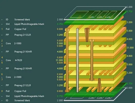
Layer stack-up is the arrangement of copper and insulating layers in a PCB, crucial for electrical performance and production compatibility. Stack-up helps control circuit noise, improve signal integrity, and reduce impedance and crosstalk, especially in high-speed layouts. A good stack-up offers the following advantages:
· Minimizes vulnerability to external noise and electromagnetic radiation.
· Balances cost-effectiveness with high signal integrity.
Key considerations for selecting stack-up include:
· Layer Count: Higher layers offer improved routing space and noise isolation.
· Signal Integrity: Layers should support stable and clean signal flow.
· Power and Ground Planes: Dedicated planes reduce impedance and noise.
· Thermal Management: Proper distribution of layers helps heat dissipation.
· EMI/EMC Control: Layer configuration reduces electromagnetic interference.
· Material Selection: PCB materials impact signal speed and impedance.
· Signal Layer Ordering: Proper arrangement reduces noise and simplifies routing.
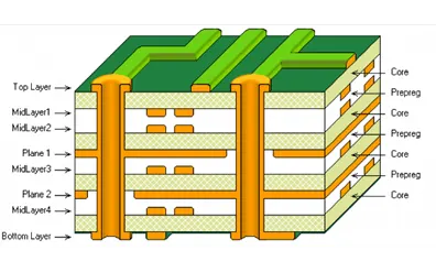
For a non-synchronous boost controller, a four-layer stack-up may be ideal, supporting ground and power planes, signal paths, feedback, and control.
2. How do you calculate the trace width, via size and trace length.
Trace Width: Calculated based on current capacity and temperature rise. The following steps and constants apply:
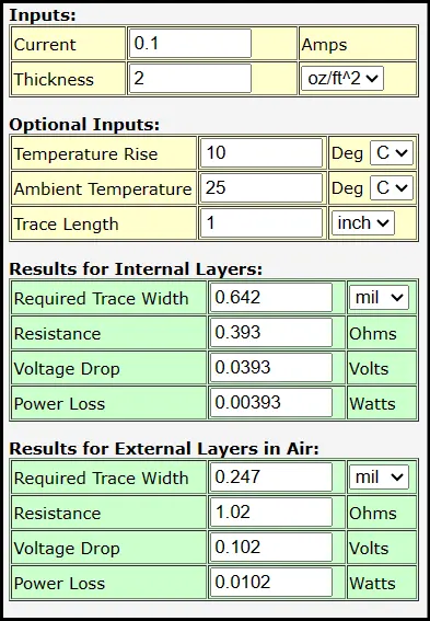
Calculate Area:
Area[mils^2] = (Current [Amps]/ (k*(Temp_Rise [deg. C]) ^b)) ^(1/c)
Then, the Width is calculated:
Width[mils] = Area[mils^2]/(Thickness[oz]*1.378[mils/oz])
For internal layers, constants are k=0.024k, b=0.44b, c=0.725. For external layers, k=0.048k, b=0.44b, c=0.725.
Following these, internal layer width is about 0.642 mils, and external layers around 0.247 mils.
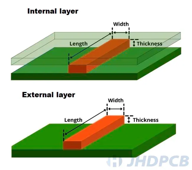
Via Size:
Via size considerations include:
· Manufacturing Cost: Larger vias reduce production cost.
· Trace Width: Pads should be larger than vias.
· Reliability: Larger pads enhance durability.
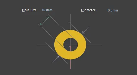
For via pad size, IPC-2222 provides minimum via dimensions based on hole diameter:
Calculate Minimum Hole Size:
Minimum Hole Size = Max Lead Diameter + Allowance
Calculate Via Pad Diameter:
L=a+2b+c
where:
· a: Finished hole diameter for external layers.
· b: Minimum annular ring size.
· c: Fabrication tolerance.
3. What all you do to avoid heating of component in a 4 layer PCB.
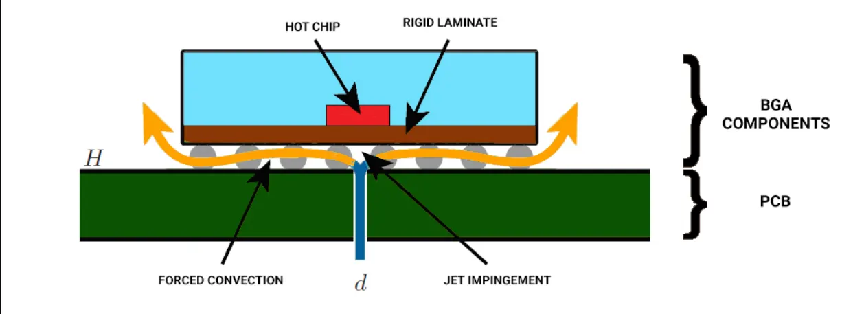
Preventing excessive heat in a 4-layer PCB requires a strategic approach:
· Thermal Via Arrays: Use arrays of thermal vias in copper-filled areas to transfer heat away from hot spots, particularly beneath power-dense components.
· Material Selection: Use materials with higher thermal conductivity to improve heat distribution.
· Heat Dissipation Techniques: Employ heat sinks, fans, or thicker copper plating where high thermal loads exist.
· Adequate Component Spacing: Maintain spacing between heat-generating components to avoid localized heating.
· Thermal Planes and Partitions: Create thermal planes with well-placed vias and partitions to distribute and dissipate heat efficiently.
· Heat Pipes: Integrate heat pipes to move heat to cooler areas of the PCB where necessary.
4. What are the advantages of a multilayer PCB?
Multilayer PCBs offer numerous advantages for complex designs:
· Higher Density: Multilayer designs support increased component density, enabling more compact and functional designs.
· Better Signal Integrity: Dedicated ground and power planes reduce electromagnetic interference, enhancing signal quality in high-speed circuits.
· Improved Power Distribution: Integrated power and ground planes ensure stable power across the board, reducing voltage drops and improving reliability.
· Enhanced Reliability: Redundant layers in a multilayer board add durability, which is essential for critical applications.
· Flexible Design Options: The additional layers offer routing flexibility, allowing designers to control impedance, minimize crosstalk, and optimize circuit layout.
· Thermal Management: Multilayer boards allow for enhanced thermal management with embedded thermal vias and conductive planes, critical for dissipating heat in high-performance applications.