Project 2 - SiC/IGBT isolated gate driver reference design with thermal diode and sensing FET
- How will you decide the layer stack up.
The first consideration for your PCB stackup is determining how many layers are needed. This includes considering signal (high speed, low speed), power (for high power boards or when power supplies are a part of your circuit) and ground layers or planes. It is highly recommended not to mix signal types on inner layers.
The circuit has
- Double-side-cooled IGBT module with integrated thermal diode for temperature monitoring and sensing FET for overcurrent protection
- Multiple redundant circuits, supply voltage monitoring, and PWM output monitoring for increased level of system safety.
- Isolated gate driver on board with a ±10-A drive strength, fast overcurrent and short-circuit protection, and analog-to-PWM sensor.
- Fault signal injection for function validation.
- Serial peripheral interface (SPI) with 12-bit ADC for accurate temperature monitoring.
So for better implementation, minimum 4 layer stack up must be needed. As there are large number of components and needed to provided redundancy for power flow, thermal sensing the components needs to be placed on top and bottom layer, which restricts the amount of routing that can be done in two layers.
So we can use two more layers for power lines,planes and ground planes.
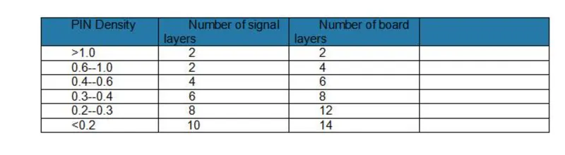
Also,for most boards, you can use the pin density to get an accurate layer count,where,
PIN density: Area of board (square inch)/ (Total number of pins on the Board/14)
After calculating the pin density, you may use a readily available lookup table to find the number of signal layers and total layers
How do you calculate the trace width, via size and trace length.
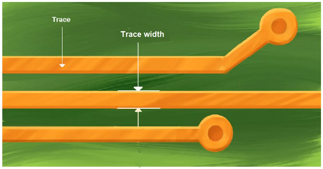
A PCB trace comprises width, thickness, and length. All these elements affect the functioning of the circuit board. Besides, it is normal to design PCBs with distinct widths based on their intended applications. For instance, traces designed for general applications, such as TTL demand smaller widths than those designed for power transmission
The trace width is basically the width of the copper foil.Miscalculating the width might burn the trace.
The trace width is determined by various factors like current, signal type, temperature, thickness, and others.
One can use many online free software tools that are available to calculate trace width, via size and trace length depending upon the application. Most important factors that decide the trace width,length are the value of current it carries, heat dissipation values, surge curent,overload current,open circuit voltage to avoid arc build up.
The best way of finding the PCB trace width is by applying the trace width equation. The formula will enable you to find the tolerable current conducted through a particular trace. Below is the IPC 2221 trace width formula:
I=k*ΔT^0.44*A^0.725
I is the current, and it is always constant. ΔT is the temperature change, and A is the cross-sectional area.
Longer traces create a high resistance, implying that length is also an important PCB trace resistance consideration. You should aim to design a small board by minimizing the length of the traces.
Trace spacing refers to the distance between two traces. Like the trace width and length, it is also an important trace resistance consideration. Importantly, trace spacing will enable you to prevent flashovers between two conductors. A flashover is a current breakdown that appears along the PCB surface or junction.
The trace resistance of a microstrip is important in determining how much power it dissipates. By determining its trace resistance, the contribution of a microstrip to the overall circuit resistance can be evaluated. This tool is designed to calculate the resistance of a microstrip trace with a copper conductor. To use it, specify the trace dimensions and the ambient temperature.
Equation
Where:
ρ=resistivity
L= length
W=trace width
T=trace height
-----------------------------------------------------------------------------------------------------------------------------------------------
What all you do to avoid heating of component in a 4 layer PCB.
Modern electronics use high power components like high-performance processors, MOSFETs, high power LEDs, IGBTs, etc. These components are made smaller but this results in the creation of thermal hotspots. High temperatures at PCB thermal hotspots could result in device failure. Hence PCB thermal management techniques must be carried out in PCBs.
Thermal performance is one of the most critical factors to consider while designing electronic products. To combat heating issues, PCB designers need to incorporate techniques that reduce the impact of heating.
The proper geometrical arrangement of components and high-current traces enables even distribution of heat. High-current traces must be routed away from thermally sensitive components such as sensors.
The thickness and width of the copper pad or traces play a significant role in PCB thermal design. Copper trace thickness should be adequate to provide a low impedance path for current passing through it.
This is because the resistance of copper traces and vias accounts for significant power loss and heat generation particularly when they bear high current density. Therefore sufficient trace width and thickness are recommended to reduce heat generation.
Heat is dissipated directly towards the top copper layer. Therefore, the top copper pad must have sufficient thickness and area to provide enough heat spreading.
If the PCB design has heat sinks in it, they are usually mounted on the bottom copper pad. Then the bottom copper pads should have sufficient coverage to allow optimum heat transfer to the heatsink.
The solder paste used to connect the component footprint with the thermal pad should be minimal. Too much solder paste under the thermal pads can result in the floating of components on a pool of molten solder during reflow.
High power components such as processors and microcontrollers should be placed at the center of the PCB. If a high power component is mounted near to the edge of the board, it will accumulate heat at the edge and raise the local temperature. But if the device is placed at the center of the board, heat will scatter over the surface in all directions. Thus the surface temperature of the PCB would be lower and dissipates easily.
The heat sink is a cooling method that transfers dissipated heat from PCB components into a cooling medium.
The cooling fan uses convective heat transferring method that offers the designer a much efficient method for getting the heat away from components.
PCB designers have two options to avoid the overflow of solder. The first one is to decrease the diameter of the via below 0.3mm. The smaller the vias, the surface tension of the liquid solder inside the via is better able to counter the force of gravity on the solder.
--------------------------------------------------------------------------------------------------------------------------------------------
Advantage of multilayer PCB
multilayer PCB is a PCB that is made with three or more conductive copper foil layers. These appear as several layers of double-sided circuit boards, laminated and glued together with layers of heat-protective insulation between them. The entire construction is arranged so that two layers are placed on the surface sides of the PCB to connect to the environment.
Benefits multilayer PCBs present include -
• Small Size: One of the most prominent and lauded benefits of using multilayer PCBs lies in their size. Because of their layered design, multilayer PCBs are inherently smaller than other PCBs with similar functionality.
• Lightweight Construction: With smaller PCBs comes less weight, especially as the multiple connectors required to interlink separate single and double-layered PCBs are eliminated in favor of a multilayered design.
• High-Quality: Due to the amount of work and planning that must go into the creation of multilayer PCBs, these types of PCBs tend to be better in quality than single and double-layer PCBs. They also tend to be more reliable as a result.
• Increased Durability: Multilayer PCBs tend to be durable by their nature. Not only do these multilayer PCBs have to withstand their own weight, but they must also be able to handle the heat and pressure used to bind them together. On top of these factors, multilayer PCBs use multiple layers of insulation between circuit layers, binding it all together with prepreg bonding agent and protective materials.
• More Powerful: Multilayer PCBs are extremely high-density assemblies, incorporating multiple layers into a single PCB. These close-quarters enable boards to be more connective, and their innate electrical properties allow them to achieve greater capacity and speed despite their smaller size.