Project 2
Project 2
Design an interleaving DC/DC converter
following specifications:
Input voltage: 45 – 60 v, Output voltage: 3 V, Output current: 100A, Efficiency > 85%
Duty cycle (D)=0.05 - 0.067, Output current =100A, Load (RL)=30m ohm, output power =300watt
input power=350watt input current=5.84 - 7.78 A losses=50watts.
Forward converter
Here it is very difficult to generate such a small duty cycle. so go for forward converter is better and The power applied to the switch in an isolated buck will be lower than in the Buck
Turns ratio of transformer (m)=(V2/V1)( here v2 is greater than 3v i.e 20v)=0.44
m*D =Np/Nd ( the transformation ratio between the primary winding and the demagnetized winding)=0.014
In order to assure the complete demagnetization of the transformer the surface under the curve during the time,
[0 DT] of V1 must be as large as the surface under the curve during the time [DT (1− D)T]
Dmax=(0.44)/(0.44+1)=0.3
Effective windings area inside the core(Ae)=(Vin min*Dmax)/(Np*fs*B)
let consider :
switching frequency (fs)=50 KHz, transformer winging factor(kp)=0.5, flux density(delta B)=0.3T, ( Kw)=0.4,
maxmimum current desity(Jmax)=450A/cm.sqr, Aw=3 cm sqr, Ae=1.81cm sqr, Deta (IL)=20% of Inductor current, Voltage ripple in output(delta V)=0.01
Forward Transformer Design:
current in transformer primary winding(Ip)=(1.2*pout)/(vin*D*efficiency)=31.37A
Number of turns in primary winding (Np)= (vin min *Dmax)/(Ae*B*f)=49.9==50 turns
Secondary turns number must be determined: Vout = V1D = (V2 −VF)D with VF the voltage drop into the D1
diode.
Ns=Np*(Vout+(vf*Dmax))/ (Vin min*Dmax)=13.33==14 turns
Tertiary turns number can be determined(Nd)=(Np*Dmax)/(1-Dmax)=21.42==22 turns
we can now calculate the optimal value of the duty cycle, we will use in our forward converter in order to comply with the specified output parameters.
D=Vout/(m*Vin)
Output Inductor Design: The output Inductor is a very important component of the forward converter circuit. Indeed it filters the AC component and delivers the DC component of the current that will supply the load.
delta IL =20A
L=(((Ns/Np)*Vin)*(1-Dmax)-Vf)*Dmax)/(delta IL*f)=3.43 uH
Output Capacitor Design: The aim of the output capacitor is to absorb the AC current component in order to prevent it from flowing through the resistance. Thus the current that flows through the output load is only a DC current. Nevertheless, the output capacitor can’t divert the entire AC current component from the output inductor. That is why if we look very accurately at the output current it still has some oscillations at the switching frequency.
C=delta (IL)/(2*Pi*f*delta (vc))=6.3 mf
Determination of the switch:
We need to know the theoretical value that can be applied to the switch. The maximum theoretical voltage applied across the switch is...
Vt=Vin(1+(Np/Nd))=196V, So I consider using the IRFBG20 Mosfet 200 V/high frequency, Indeed we must choose a MOSFET with a maximum voltage higher than the one given by calculation and simulation.
switch power loss =Rds*I=0.047*31.7=1.9watt
Choice of the diodes: Aims of D1 and D2, DM Diodes are to prevent negative current to flow through transformer secondary and to allow freewheeling during demagnetization time.
Theoretical voltage into the secondary is V2=(Ns/Np)*Vin= 14.4 , Vd1<14.4, Vdm=2.5*Vin=150V.
Thus I choose for D2 and Dm ,MBR735,RF2001NS2D respectively.id1(avg)=0.12A,Id2(AVG)=0.17A,Idm(AVG)=.03A
diodes power loss=10.48Watt.
Total losses: diode power loss+switching power losses+transformer losses=14.3watt
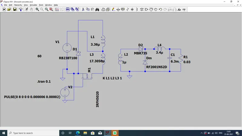
schematic diagram of forward converter:
simulation results of forward converter: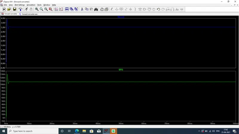
Two DC/AC H-bridge inverters
Output voltage Amplitude (Fundamental) Vo,1 = Ma * Vdc
Vdc - Input DC voltage=220V
Vo,1 - Fundamental output AC voltage amplitude=170V
Ma=0.772
Amplitude Modulation ratio (Ma) : Ma = Ar / Ac
Ar - Reference Sine wave Amplitude=0.772v
Ac - Carrier wave Amplitude=1
Frequency Modulation ratio (Mf) : Mf = fc / fr
fc- Carrier wave frequency=1M Hz
fr- Reference wave frequency=50 Hz
Mf=20K Hz
Load KVA: KVA=sqrt((kw*kw)+(kvar*kvar))= 5.38KVA.
V-out rms==121V
I-out rms=44.46A
Impedence: Z=V\I=2.721 ohm
Resistive load:
active power (p)=I*I*R=5000watt
R==2.52 ohm
reactive load :
XL==1.052 ohm
inductor value(L)=3.35mH
LCL Filter:
L1=6.18*e-4 mH
L2=0.000173H
C=4.35*e-5 F
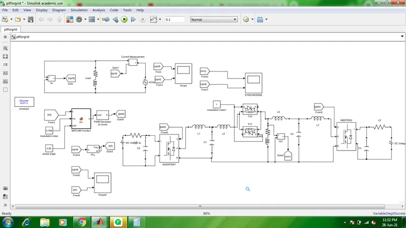
Schematic diagram of parallel inverter connection:
function code:
function a = fcn(x,ma,shift)
shiftk =(shift*pi)/180;
a=(ma*(sin((x)+shiftk)));
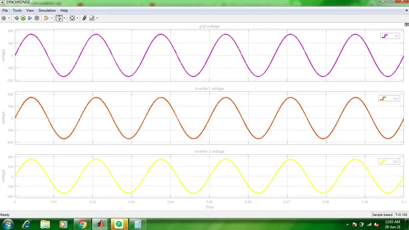
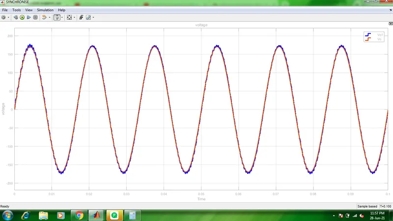
inverter1 voltage comparing with microgrid voltageL:
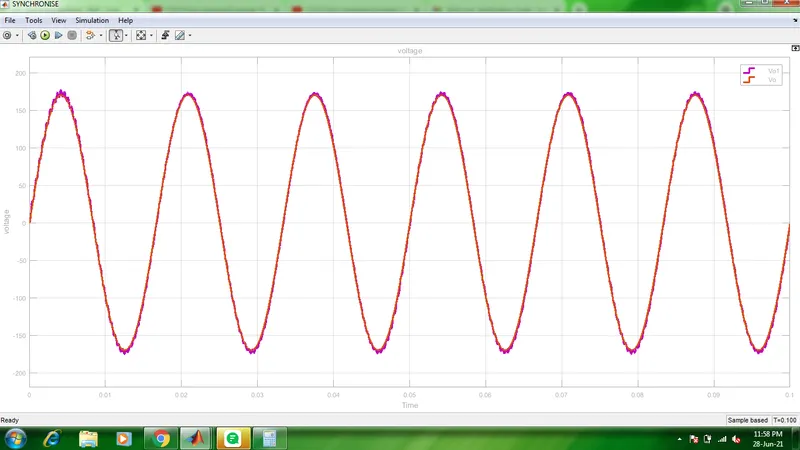
inverter2 voltage comparing with microgrid voltage:
comparision of inverter1 ,invert2,grid voltages: