Project 1- Traffic Jam Assistant Feature
Traffic Jam Assistant Feature-
Traffic Jam Assistant is one of the most common feature in Advanced Driver Assistance System. Traffic Jam Assistant helps the driver arrive more relaxed at their destination, even in dense traffic or in traffic jams. Traffic Jam Assistant system helps to avoid rear end collisions in dense traffic conditions & traffic jams. In Traffic jams, the vehicle takes over driving off, acceleration, braking and steering within same lane.
Problem Statement:
To develop one specific requirement of Traffic Jam Assistant algorithm which would predominantly feature in the IPC algorithm.Please note that the whole Traffic Jam Assistant is a very huge algorithm & only one small part of the logic is implemented here. Idea is to familiarize with concepts of Model Based Development in MATLAB Environment. The Project must be done keeping in mind the following processes & steps.
- This model must be developed in MATLAB Simulink as per MBD guidelines.
- Code Generation Profile must be in Embedded Coder.
- Simulink Data Dictionary must be created for the model & must be linked to the model.
- Model Advisor Report is mandatory & this will be followed by Code Generation.
Input Signals:
Name of the Signal | Data Type | Range |
Input_Voltage | uint8 | 0 - 255 |
Input_Switch | boolean | 0 – 1 |
Enable_Display | uint8 | 0 - 255 |
Output Signal:
Name of the Signal | Data Type | Range |
Output_Display | uint8 | 0 - 255 |
Calibration Signals:
Name of the Signal | Data Type | Range | Initial Value |
VOLTAGE_MINIMUM_RANGE | uint8 | 0 – 255 | 30 |
VOLTAGE_MAXIMUM_RANGE | uint8 | 0 – 255 | 50 |
OFF_MODE | uint8 | 0 – 255 | 2 |
ON_MODE | uint8 | 0 – 255 | 1 |
STANDBY_MODE | uint8 | 0 – 255 | 3 |
INTERRUPT_1 | boolean | 0 – 1 | 1 |
INTERRUPT_2 | boolean | 0 - 1 | 1 |
NO_DISPLAY | uint8 | 0 – 255 | 0 |
Local Signal:
Name of the Signal | Data Type | Range |
Optimum_Voltage | boolean | 0 - 1 |
Requirement No 1:
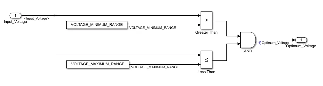
- Input Signal “Input_Voltage” is compared against voltage values “VOLTAGE_MINIMUM_RANGE” & “VOLTAGE_MAXIMUM_RANGE”.
- Incoming input signal “Input_Voltage” must be greater than – equal to “VOLTAGE_MINIMUM_RANGE” and less than – equal to “VOLTAGE_MAXIMUM_RANGE”.
- Output signal from here is “Optimum_Voltage” which will be one of the inputs to the subsystem “DisplayUnit”.
Requirement No 2 (DisplayUnit Subsystem):
- Input Signals are “Optimum_Voltage”, “Input_Switch”,“Enable_Display”. Signal “Enable_Display” must be saturated between the range 0 – 7. Output signal from the subsystem is “Output_Display”.
- Input Signal “Enable_Display” is compared against pre – defined set of values in a multiport switch. Total data ports in the multiport switch is 5.
- Multiport switch inputs 1 & 2 is connected to calibration signal “ON_MODE”, Multiport switch inputs 3 & 4 is connected to calibration signal “OFF_MODE” while Multiport switch input 5 is connected to calibration signal “STANDBY_MODE”.
- The output from Multiport switch is connected to the first input port of the Switch block. The third input port of the Switch block is connected to the calibration signal “NO_DISPLAY”.
- Meanwhile NOT value of input signal “Input_Switch” is compared in an AND gate against input signal “Optimum_Voltage” and the output from comparing if calibration signals “INTERRUPT_1” & “INTERRUPT_2” are equal. The output of the AND gate is the second input of the switch block.
- The output from the switch block is “Output_Display”.
Simulink Model-
As per Requirement No 1:
- Input Signal “Input_Voltage” is compared against voltage values “VOLTAGE_MINIMUM_RANGE” & “VOLTAGE_MAXIMUM_RANGE”.
- Incoming input signal “Input_Voltage” must be greater than – equal to “VOLTAGE_MINIMUM_RANGE” and less than – equal to “VOLTAGE_MAXIMUM_RANGE”.
- Output signal from here is “Optimum_Voltage” which will be one of the inputs to the subsystem “DisplayUnit”.
Steps-
- Take Input block and name it as Input_Voltage
- Now we have compare this Input_Voltage signal with two constant values i.e. VOLTAGE_MINIMUM_RANGE & VOLTAGE_MAXIMUM_RANGE hence take two relational operator blocks.
- To relational operator block 1 connect the upper port to incomming signal and another port to the predetermined constant value VOLTAGE_MINIMUM_RANGE.
- To relational operator block 2 connect the upper port to incomming signal and another port to the predetermined constant value VOLTAGE_MAXIMUM_RANGE.
- Then output of these relational operators is given to the AND gate. and output of AND gate named as Optimum_Voltage is provided to next subsystem.
As per Requirement No 2 (DisplayUnit Subsystem):
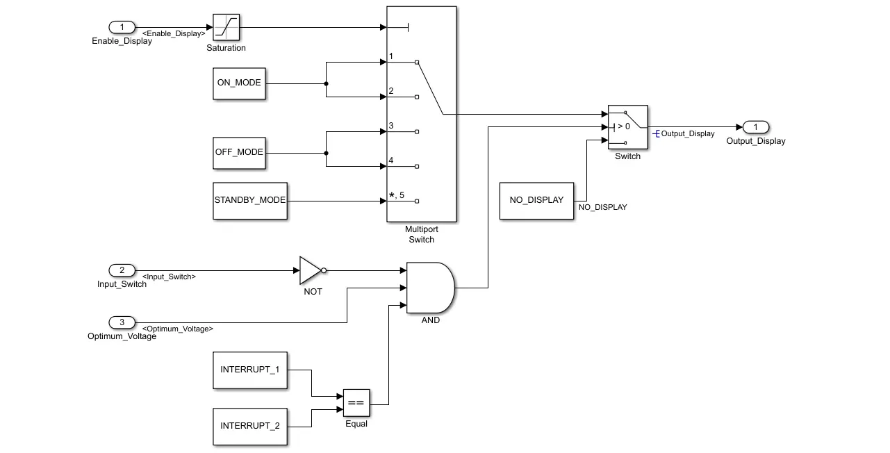
- Input Signals are “Optimum_Voltage”, “Input_Switch”,“Enable_Display”. Signal “Enable_Display” must be saturated between the range 0 – 7. Output signal from the subsystem is “Output_Display”.
- Input Signal “Enable_Display” is compared against pre – defined set of values in a multiport switch. Total data ports in the multiport switch is 5.
- Multiport switch inputs 1 & 2 is connected to calibration signal “ON_MODE”, Multiport switch inputs 3 & 4 is connected to calibration signal “OFF_MODE” while Multiport switch input 5 is connected to calibration signal “STANDBY_MODE”.
- The output from Multiport switch is connected to the first input port of the Switch block. The third input port of the Switch block is connected to the calibration signal “NO_DISPLAY”.
- Meanwhile NOT value of input signal “Input_Switch” is compared in an AND gate against input signal “Optimum_Voltage” and the output from comparing if calibration signals “INTERRUPT_1” & “INTERRUPT_2” are equal. The output of the AND gate is the second input of the switch block.
- The output from the switch block is “Output_Display”.
Steps -
- Here there are 3 main inputes i.e. outout of subsystem1 (Optimum_Voltage), Input_Switch, Enable_Display, and one output i.e. Output_Display.
- Take a saturation block, input to this block is Enable_Display while output is connected to main port of multiport switch.
- Connect calibration signal blocks as mentioned in requirement.
- Output of the multiport switch is given to the switch block.
- Second input to this shitch is a output signal from AND gate. 1st input to this AND gate is NOT signal of Input_Switch, 2nd input to AND gate is Optimum _Voltage.
- Third input to the AND gate a result of comparision between two signals.
- Output of this subsystem is Output_Display.
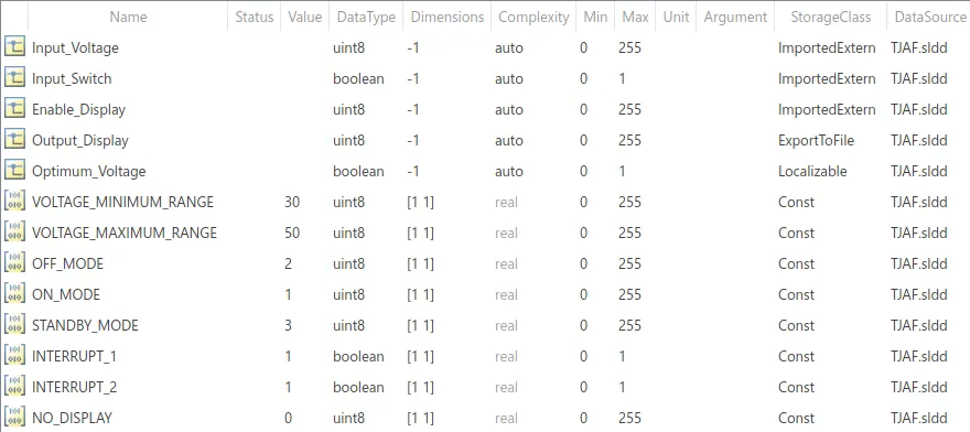
Simulink Data Dictionary creation-
As per given data SLDD is created as following-
Model Advisor Report-
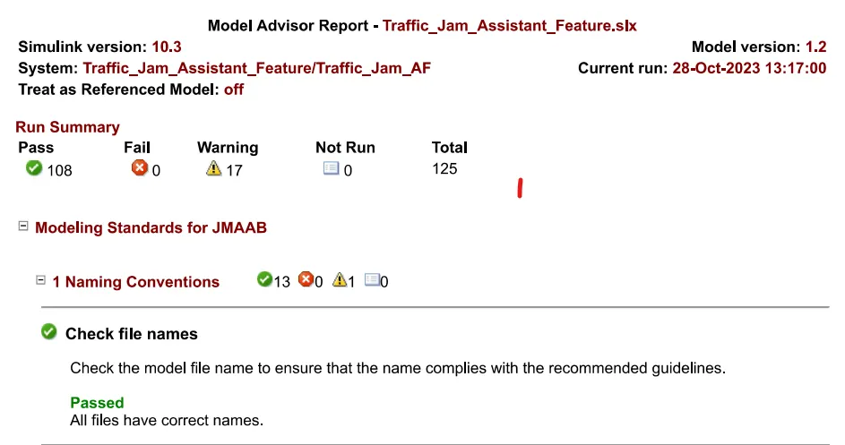
After complition of modeling we have to create Model Advisor Report for the perticular model.
Steps-
- Click on 'Modeling' option.
- In upper left corner there is a option with green mark 'Model Advisor' click on it.
- A window will get open, select the model name.
- Click on 'By product',
- Then selct 'Modeling standerd for MAB' & 'Modeling standards for JMAB'.
- Click on 'Run selected checks'.
- Advisor report will gate created and displayed on the window.
Code Generation-
Steps-
- Click on 'Modeling' option.
- Click on Model srettings.
- In 'Solver' go to 'Solver selection', select type as 'fixed step' and select 'Solver' as 'Discrete'.
- In code generation go to 'System target file' and edit the file name as 'ert.tlc'.
- Apply and click on 'OK'.
- Then click on Apps, go to 'Embedded Coder'.
- And click on 'Build'.
- All the generated code files will be stored at your model saved location.