Project 1 - 40-V to 80-V adjustable output voltage boost reference design for LIDAR applications
Project 1 - 40-V to 80-V adjustable output voltage boost reference design for LIDAR applications
Description: To design a non-synchronous boost controller to provide an adjustable output of between 40 V and 80 V capable of delivering a maximum of 100 mA of current to the load. This is an automotive design intended to power various applications such as LiDAR systems, which require an adjustable voltage supply.
Question:
1. How will you decide the layer stack up.
2. How do you calculate the trace width, via size and trace length.
3. What is the drawback of having 2 layers PCB?
1. How will you decide the layer stack up.
Layer stack-up is the arrangement of copper and insulating layers in a PCB, crucial for electrical performance and production compatibility. Stack-up helps control circuit noise, improve signal integrity, and reduce impedance and crosstalk, especially in high-speed layouts. A good stack-up offers the following advantages:
· Minimizes vulnerability to external noise and electromagnetic radiation.
· Balances cost-effectiveness with high signal integrity.
Key considerations for selecting stack-up include:
· Layer Count: Higher layers offer improved routing space and noise isolation.
· Signal Integrity: Layers should support stable and clean signal flow.
· Power and Ground Planes: Dedicated planes reduce impedance and noise.
· Thermal Management: Proper distribution of layers helps heat dissipation.
· EMI/EMC Control: Layer configuration reduces electromagnetic interference.
· Material Selection: PCB materials impact signal speed and impedance.
· Signal Layer Ordering: Proper arrangement reduces noise and simplifies routing.
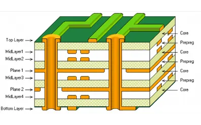
For a non-synchronous boost controller, a four-layer stack-up may be ideal, supporting ground and power planes, signal paths, feedback, and control.
2. How do you calculate the trace width, via size and trace length.
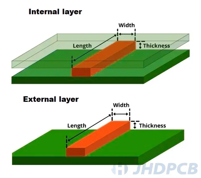
Trace Width: Calculated based on current capacity and temperature rise. The following steps and constants apply:
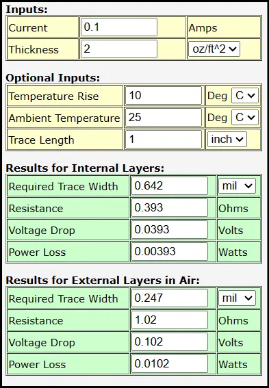
Calculate Area:
Area[mils^2] = (Current [Amps]/ (k*(Temp_Rise [deg. C]) ^b)) ^(1/c)
Then, the Width is calculated:
Width[mils] = Area[mils^2]/(Thickness[oz]*1.378[mils/oz])
For internal layers, constants are k=0.024k, b=0.44b, c=0.725. For external layers, k=0.048k, b=0.44b, c=0.725.
Following these, internal layer width is about 0.642 mils, and external layers around 0.247 mils.
Via Size:
Via size considerations include:
· Manufacturing Cost: Larger vias reduce production cost.
· Trace Width: Pads should be larger than vias.
· Reliability: Larger pads enhance durability.
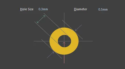
For via pad size, IPC-2222 provides minimum via dimensions based on hole diameter:
Calculate Minimum Hole Size:
Minimum Hole Size = Max Lead Diameter + Allowance
Calculate Via Pad Diameter:
L=a+2b+c
where:
· a: Finished hole diameter for external layers.
· b: Minimum annular ring size.
· c: Fabrication tolerance.
3. Drawbacks of a 2-Layer PCB
· Space and Routing Limitations: Reduced space for components and routing can affect performance.
· Signal Integrity Challenges: More prone to crosstalk and noise.
· Size and Weight: Larger and heavier, impacting portability.
· Design Constraints: Limited functionality and scalability.
· Higher EMI Potential: Simplistic design can introduce electromagnetic interference.