Project 1 - 40-V to 80-V adjustable output voltage boost reference design for LIDAR applications
- How will you decide the layer stack up.
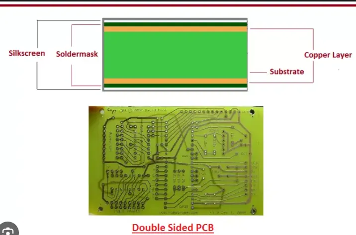
PCB layer stack-up, also called layer build-up, is the arrangement of insulating layers and conductive layers (copper layers) that make up the PCB before PCB layout design. Several insulating layers and copper layers are stacked together through the “prepreg” to generate a multiple-layered PCB.
- The Layer count is defined by Rounting constraint, Density, Package type, Power delivery etc
-How ever the stackup layer is more concerned with the electrical type of each layer in the PCB.
-For maximum efficiency and minimum losses and EMI, it is important to plan the right stack up of layers before starting the fabrication process. 4-layer PCB is the most common stack-up arrangement used in modern electronics.
- For such a simple circuit a 2 or 4 layer stackup could be choosen. For maximum efficiency and minimum losses and EMI, a 4 layer stackup will be chooseny, since a 2 and 4 layer stackup have little cost difference but 4 layer stackup offer more efficiency.

2.How do you calculate the trace width, via size and trace length.
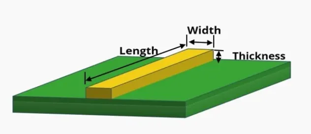
- Trace widths are often measured in mils, or thousands of an inch. A standard trace width for an ordinary signal (no special requirements) may be in the 7-12 mil range and be as long as a few inches, but there are many things that should be considered when defining the width and length of a trace.
The Trace Width is calculated: Width[mils] = Area[mils²] / ( Thickness[oz] * 1.378[mils/oz] )
- When it comes to the Via size, we have to take into concidaration the via diameter and the via drill diameter. The Via drill is the finished size of the actual hole. diameter is the outer diameter of the copper surrounding the hole. The annular ring of the via will be the (diameter-drill)/2.
- PCB trace length matching is exactly as its name suggests: you are matching the lengths of two or more PCB traces as they are routed across a board. These traces could be one of the following: Multiple single-ended traces routed in parallel. Each end of a differential pair. For example calculating the maximum skew of the trace length for all the signals? So, for strip lines, the maximum skew should be less than +/- (20.825/(85*SQT(4))=+/-0.1225 in = +/- 122.5 mil. For microstrips, the maximum skew should be less than +/- (20.825/(85*SQT(2.92)) = +/-0.1433 in = +/- 143.3 mil.
3.What is the drawback of having 2 layers PCB?
The main drawback of 2 Layer PCBs is that they are not as durable as other types of PCBs.It can be difficult to route all the necessary traces, especially in complex designs or designs with high component density. this can lead to signsl integrity issues,as well as difficulty in fitting all the necessary components onto the board.