Project 1 - 40-V to 80-V adjustable output voltage boost reference design for LIDAR applications
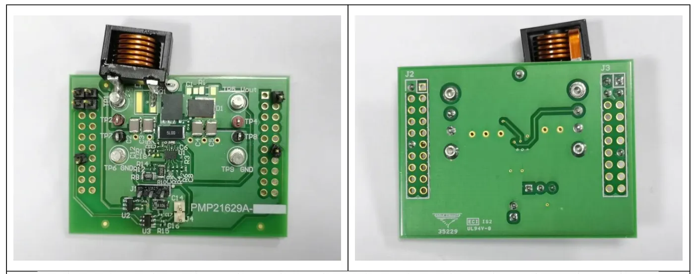
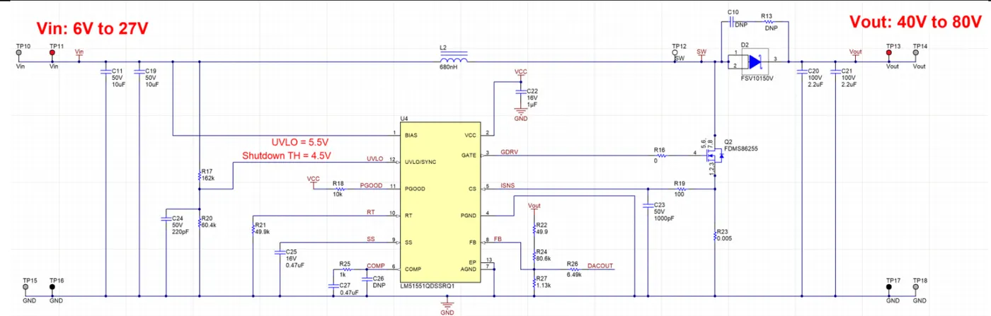
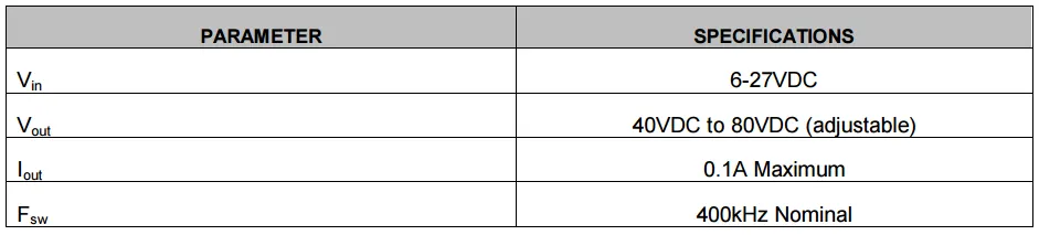
Description: To design a non-synchronous boost controller to provide an adjustable output of between 40 V and 80 V capable of delivering a maximum of 100 mA of current to the load. This is an automotive design intended to power various applications such as LiDAR systems, which require an adjustable voltage supply.
Schematic is shown:
Question:
1. How will you decide on the layer stack-up?
Deciding on the layer stack-up for a PCB involves careful consideration of various factors such as signal integrity, power distribution, electromagnetic interference (EMI), manufacturability, cost etc.
Signal Integrity:
Signal integrity refers to the quality of signals transmitted across the PCB, including factors like signal loss, reflections, and crosstalk. To maintain good signal integrity, we should minimize signal traces' length and impedance mismatches and provide a solid reference plane (usually ground) for signal return paths. Using multiple signal layers and dedicated ground planes can help achieve this.
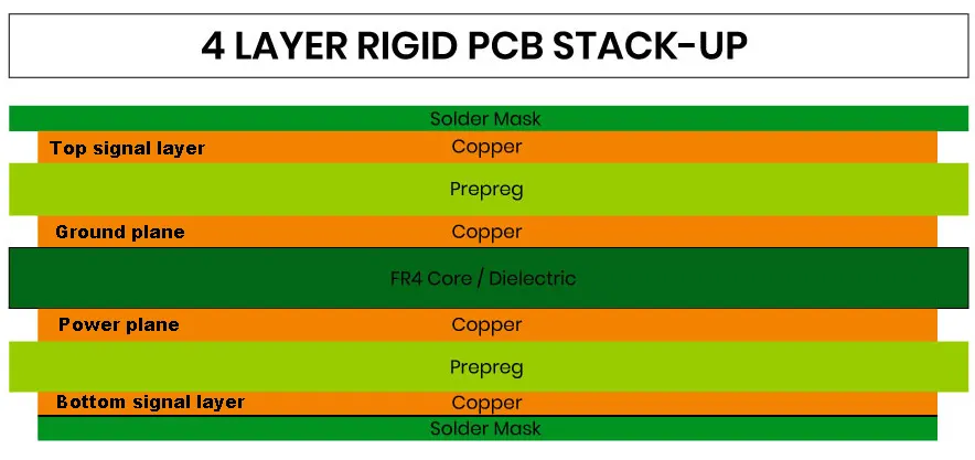
Power Distribution: Power distribution is crucial for ensuring stable voltage levels across the PCB, especially for sensitive components like the boost controller and LiDAR systems. Dedicated power planes can efficiently distribute power to components while minimizing voltage drops and noise. The layer stack-up should include at least one power plane and one ground plane to provide a stable power distribution network.
EMI Considerations: Electromagnetic interference (EMI) can negatively affect the performance of sensitive electronic components and can also cause regulatory compliance issues in automotive applications. Properly designed layer stack-ups can help mitigate EMI by providing shielding between signal traces and by incorporating ground planes to act as shields against external interference.
Manufacturability: The chosen layer stack-up should be manufacturable with the selected fabrication process and technology. Complex layer stack-ups may increase manufacturing costs and complexity, so it's essential to balance design requirements with manufacturing feasibility.
Cost: Each additional layer in the PCB stack-up adds to the manufacturing cost. Therefore, it's essential to consider the cost implications of the chosen layer stack-up, balancing the performance requirements with cost constraints.
For this design of Boost converter for LiDAR application, I would design a 4-layered PCB. In this design, the average maximum voltage is 80V and the average current would be 100mA.
2. How do you calculate the trace width, via size and trace length?
Trace width calculation:
Determine the Maximum Current: Determine the maximum current the trace will carry based on the circuit. The average current is 100mA.
Select a Maximum Temperature Rise: Determine the maximum allowable temperature rise for the trace, typically based on the PCB material's thermal characteristics.
Calculate Trace Width: Use an appropriate formula or online calculator to calculate the trace width required to carry the maximum current without exceeding the maximum temperature rise. IPC-2221 provides empirical formulas for calculating trace width based on current carrying capacity and temperature rise.
Via calculation:
Determine Via Size: The via size should be chosen to accommodate the required trace width and to provide low-impedance connections between layers. The via diameter and pad size depend on the current carrying capacity and the number of vias required. We can use the Saturn PCB design tool for it.
Trace length calculation:
Calculate Trace Length: The trace length is determined by the physical layout of your PCB and the connections between components. Ensure that the trace length meets signal timing requirements and minimizes signal distortion for high-speed signals.
3. What is the drawback of having 2 layers of PCB?
The drawbacks of using a 2-layer PCB for this application are:
Limited Routing Space: With only two layers, routing traces become more challenging, especially for complex designs with many components.
Signal Integrity Issues: Two-layer PCBs may suffer from signal integrity problems like crosstalk and electromagnetic interference (EMI) due to inadequate isolation between signal traces and lack of proper ground planes.
Poor Power Distribution: Without dedicated power and ground planes, distributing power to components and maintaining stable voltage levels across the board can be difficult.
Reduced Design Flexibility: With fewer layers, it's harder to implement advanced routing techniques and impedance matching, which are crucial for high-frequency automotive applications like LiDAR systems.