Project 1
A) Buck CCM, Input Voltage 40-50 V , Output Voltage 30 V, Power level 500W
BUCK CONVERTER DESIGN AND SIMULATION
A buck converter is a DC to DC converter with an output voltage less than the source voltage. It is sometimes called a step-down converter since it "steps down" the source voltage.
A buck converter using a power MOSFET is shown below.
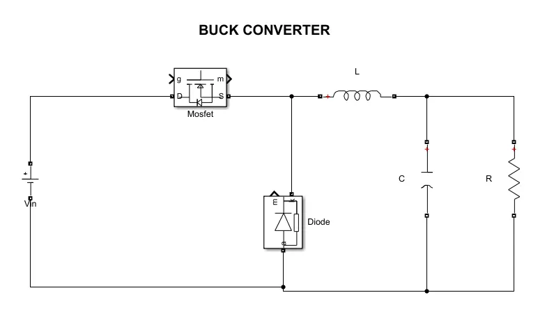
Working
The working of buck converter can be divided into two modes, Mode 1 and Mode 2. The working of these modes is explained below.
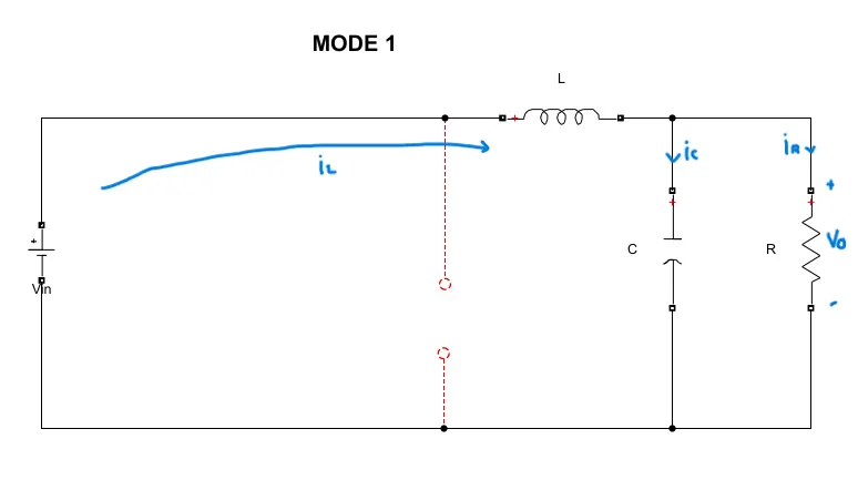
Mode 1( Switch is ON):
Mode 1 begins when Mosfet is on, Diode become non conducting. The input current rises and flows through Mosfet, inductor L , the Mosfet, capacitor C, and load(R). Here the inductor become energized.
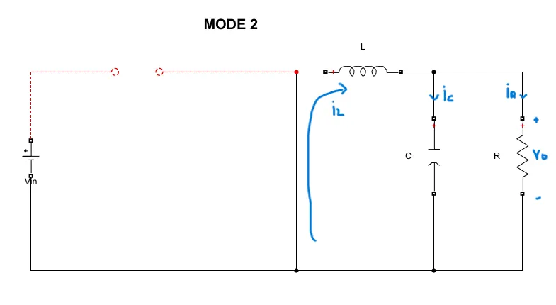
Mode 2( Switch is OFF):
Mode 2 begins when mosfet is switched off, Since inductor need to maintain its current direction,The stored energy in the inductor will flow throught the load and diode become conducting.
During this time inductor current falls until the next cycle and the energy stored in inductor L flows through the load.
The circuit of these modes are given below:
Design
Step 1-Finding the Voltage ratio
The Average inductor voltage is zero, there fore we can write
VL = (von*DT + voff*(1-D)T)/T = 0---------------(1) where D = Duty ratio
by analyzing the voltage waveform of inductor we can write von= Vin - Vout and voff = - Vout
substituting the value in equation (1)
.'. (Vin - Vout)*DT + (- Vout)*(1-D)T) = 0
=>Voltage ratio, Vout/Vin = D------------(2)
Step 2 - Design of converter inductor
Inductor voltage vL can be written as vL = L*Delta_IL/Delta_t
During ON time , vL = Vin - Vout , Delta_t = DT ,
Delta_ILon = (Vin - Vout)*DT/L-----------(3)
During OFF time, vL = - Vout, Delta_t = (1-D)T
Delta_ILoff = (-Vout)*(1-D)T)/L-----------(4)
from the diagram of boost converter we get IL = IR -----(5) since Ic = 0
The maximum inductor ILmax is given by ILmax = IL + Delta_IL/2
similarly ILmin = IL - Delta_IL/2
To make sure current in inductor is continous, ILmin >0
=> IL - Delta_IL/2 > 0
=> Lmin>= ((1-D)*R)/2*fs------(6)
Also from Eq 4 we can write
L = (Vout*(1-D))/(fs*Delta_IL)--------(7)
Step 3 - Design of converter Capacitor
Capacitance of a capacitor is given C = Q/Vout where Q is charge
=> Delta_Q = C*Delta_Vout--------(8)
Change in charge is the area under the curve for capacitor current
Thus Delta_Q = (1/2)*(T/2)*(Delta_IL/2)-----(9)
Substituting Delta_IL and equating (8) and (9) we get
Cout = (1-D)/(8*L*fs^2*(Delta_Vout/Vo))-----(10)
Components Calculation
Given Vin = 40 - 50 V , Vout = 30 v, Power P = 500W
assume Vin = 40 v, switching frequency fs = 50kHz
Eq (2) => Duty Ratio = D = Vout/Vin
D = 30/40
D = 0.75
Load Resistance R = Vout^2/P
R = 30^2/500
R = 1.8 ohm
IL = Io = P/Vout
IL = 16.66
Let design for 10% ripple in inductor current
Delta_IL = 10% of IL = 1.66
inductance L >= (Vout*(1-D)/(fs*Delta_IL) = 90.36
For to get CCM we choose L = 91uH
Capacitance C = (1-D)/(8*L*fs^2*(Delta_Vout/Vo))
Let assume output voltage ripple is 2%
=> C =(1- 0.75)/(8*91uH*50000*50000*0.02)
C = 6.86 uF
Model
With above information we built a model in simulink and analyzed the response as shown below
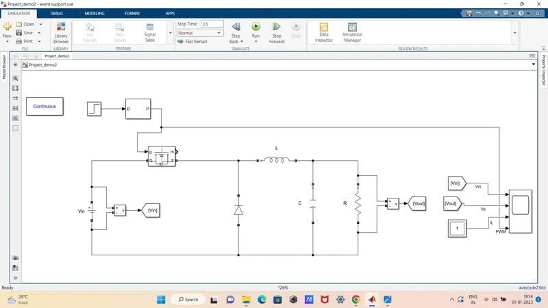
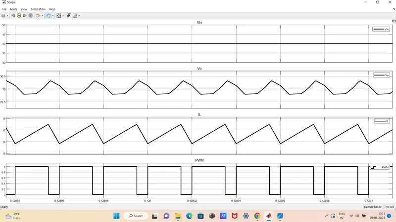
From the above response we understood that we getting the output as we expected, so we can say our choosen components value is correct. The above model is a open loop circuit and above simulation is done for ideal case. But we know there is more non idealities in the converter so we need to control the converter in order to meet the desirable specification. Thus feedback control is neccessary to achieve the desired output voltage.
Feedback control of Buck converter
The figure shows the feedback control of Buck converter.
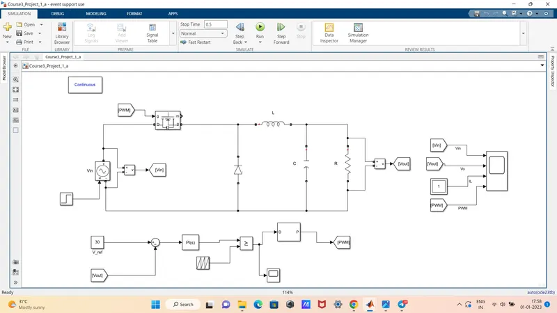
Converters system needs to be controlled in order to meet the desired specifictaions. Feedback control is neccessary to achieve the desired output voltage. In above case we are regulating the duty ratio of the converter in order to have output voltage tracking the reference voltage signal.
Here we use PID controller .The controller in this system need to met following requirements
- Output voltage to be acurately regulated
- Output voltage is insensible to disturbance
- Stable feedback system.
- etc..
Using voltage control loop, That is an error signal is made from V_ref and Vout and it is given PI controller. The signal is then compared with a repeating signal to get required switching signal.
The following are the components and their parameters used to design the above circuit.
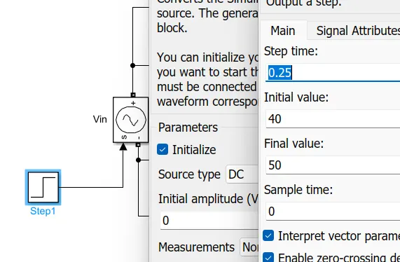
1. DC Source Voltage:
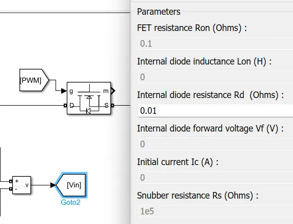
2. MOSFET
3. Inductor
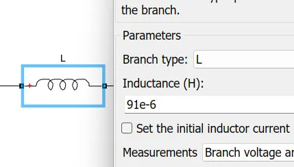
4. Capacitor
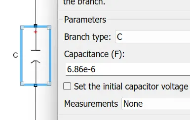
5. Load Resistor
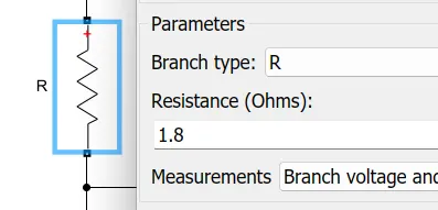
7. PI controller
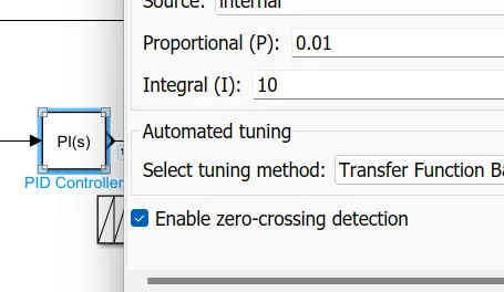
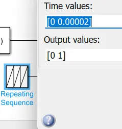
8. Repeating sequence
Result
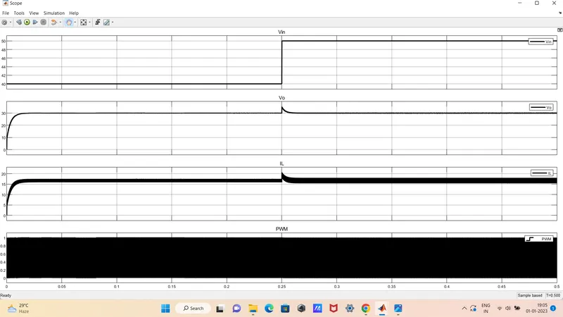
After running the simulation for 0.5 sec, we get the following output waveforms
Zoomed in:
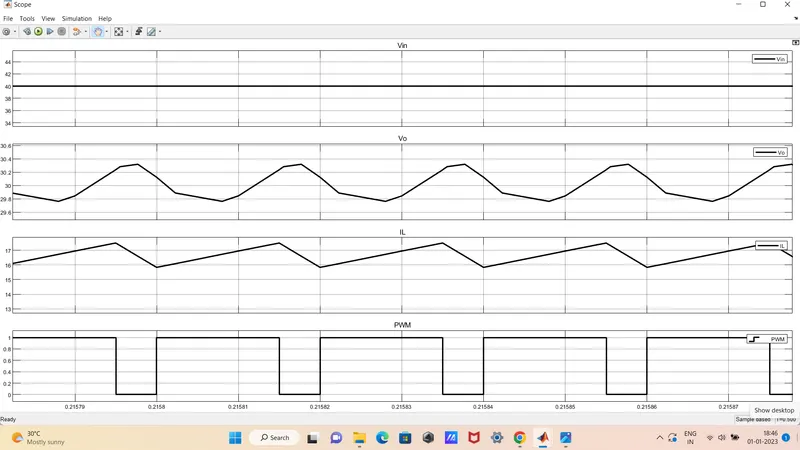
a) Before input disturbance
b) At input disturbance
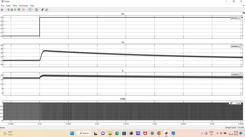
c) after input disturbance
From the above we understood that even though we made a input disturbance at t = 0.25 sec , our system given us the required output. There is small oscillation at the disturbant point but it is less as compared to initial stage.
Conclusion:
Thus, the design and simulation of a buck converter is performed and analyized the response.
B) Boost CCM , Input Voltage 20-30 V , Output Voltage 40 V, Power level 600W
BOOST CONVERTER DESIGN AND SIMULATION
A boost converter is a DC to DC converter with an output voltage greater than the source voltage. It is sometimes called a step-up converter since it "steps up" the source voltage.
A boost converter using a power MOSFET is shown below.
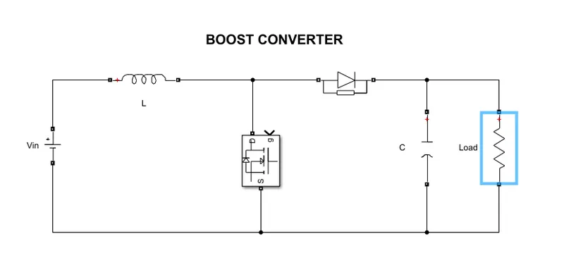
Working
The working of boost converter can be divided into two modes, Mode 1 and Mode 2. The working of these modes is explained below.
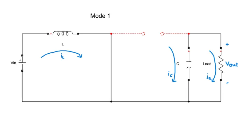
Mode 1( Switch is ON):
Mode 1 begins when Mosfet is on, The input current rises and flows through inductor L and the Mosfet.
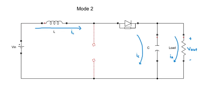
Mode 2( Switch is OFF):
Mode 2 begins when mosfet is switched off, The input current now flows through inductor L, capacitor C, load, and diode.
During this time inductor current falls until the next cycle and the energy stored in inductor L flows through the load.
The circuit of these modes are given below:
Design
Step 1-Finding the Voltage ratio
The Average inductor voltage is zero, there fore we can write
VL = (von*DT + voff*(1-D)T)/T = 0---------------(1) where D = Duty ratio
by analyzing the voltage waveform of inductor we can write von= Vin and voff = Vin - Vout
substituting the value in equation (1)
.'. Vin*DT + (Vin - Vout)*(1-D)T) = 0
=>Voltage ratio, Vout/Vin = 1/(1-D) ------------(2)
Step 2 - Design of converter inductor
Inductor voltage vL can be written as vL = L*Delta_IL/Delta_t
During ON time , vL = Vin , Delta_t = DT ,
Delta_ILon = Vin*DT/L-----------(3)
During OFF time, vL = Vin - Vout, Delta_t = (1-D)T
Delta_ILoff = ((Vin-Vout)*(1-D)T)/L-----------(4)
from the diagram boost converter we get Iin = IL
=> IL = IR/(1-D) -----(5) since Vout/Vin = 1/(1-D)
The maximum inductor ILmax is given by ILmax = IL + Delta_IL/2
similarly ILmin = IL - Delta_IL/2
To make sure current in inductor is continous, ILmin >0
=> IL - Delta_IL/2 > 0
=> Lmin>= (D*(1-D)^2*R)/2*fs------(6)
Also from Eq 3 we can write
L = (Vin*D)/(fs*Delta_IL)--------(7)
Step 3 - Design of converter Capacitor
Capacitance of a capacitor is given C = Q/Vout where Q is charge
=> Delta_Q = C*Delta_Vout--------(8)
Change in charge is the area under the curve for capacitor current
Thus Delta_Q = IR *DT where IR is the output current
=>Delta_Q = (Vout/R)*DT-------(9)
equating (8) and (9)
Cout = D/(R*fs*(Delta_Vout/Vo))-----(10)
Components Calculation
Given Vin = 20 - 30 V , Vout = 40 v, Power P = 600W
assume Vin = 25 v, switching frequency fs = 50kHz
Eq (2) => Duty Ratio = D = 1 - Vin/Vout
D = 1 - 25/40
D = 0.375
Load Resistance R = Vout^2/P
R = 40^2/600
R = 2.66 ohm
IL = Vout/R(1-D) =Vin/R(1-D)^2
IL = 24.06
Let design for 10% ripple in inductor current
Delta_IL = 10% of IL = 2.4
inductance L >= (Vin*D)/(fs*Delta_IL)
L = 80uH
Capacitance C = D/(R*fs*(Delta_Vout/Vo))
Let assume output voltage ripple is 4%
=> C = 0.375/(2.66*50000*0.04)
C = 70.48 uF
Model
With above information we built a model in simulink and analyzed the response as shown below
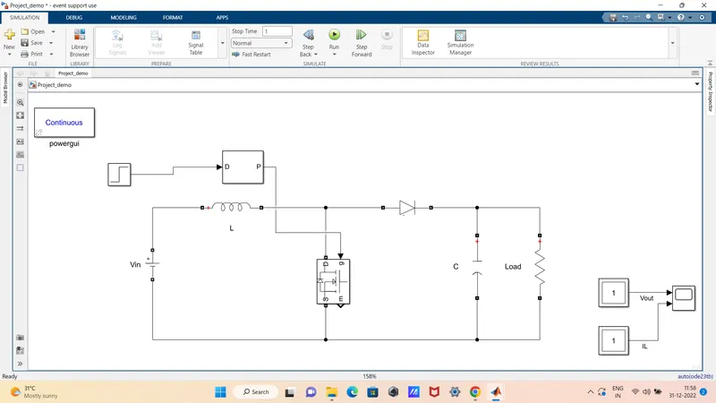
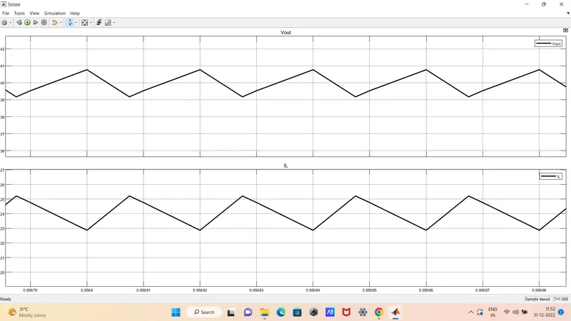
From the above response we understood that we getting the output as we expected, so we can say our choosen components value is correct. The above model is a open loop circuit and above simulation is done for ideal case. But we know there is more non idealities in the converter so we need to control the converter in order to meet the desirable specification. Thus feedback control is neccessary to achieve the desired output voltage.
Feedback control of Boost converter
The figure shows the feedback control of Boost converter.
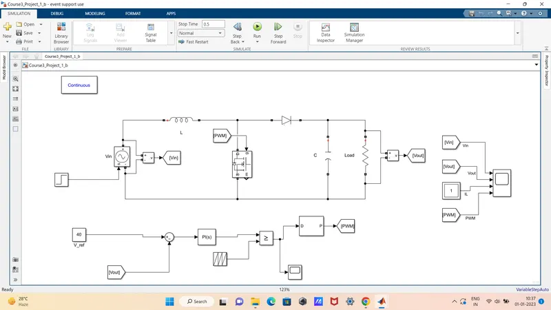
Converters system needs to be controlled in order to meet the desired specifictaions. Feedback control is neccessary to achieve the desired output voltage. In above case we are regulating the duty ratio of the converter in order to have output voltage tracking the reference voltage signal.
Here we use PID controller .The controller in this system need to met following requirements
- Output voltage to be acurately regulated
- Output voltage is insensible to disturbance
- Stable feedback system.
- etc..
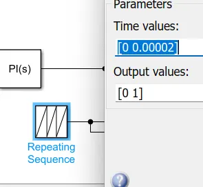
Using voltage control loop, That is an error signal is made from V_ref and Vout and it is given PI controller. The signal is then compared with a repeating signal to get required switching signal.
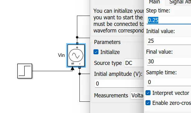
The following are the components and their parameters used to design the above circuit.
1. DC Source Voltage:
2. Inductor:
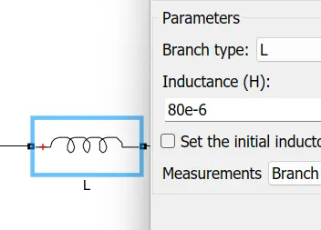
3. MOSFET:
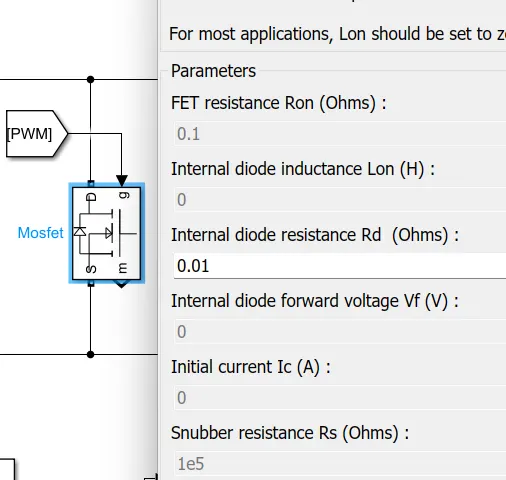
4. Filter Capacitor:
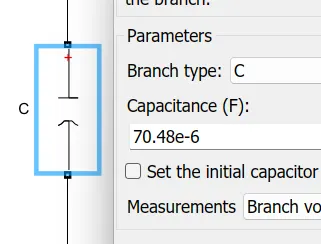
6. Load Resistor:
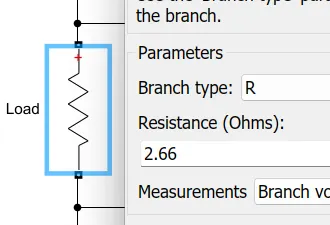
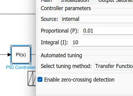
7. PI controller
8. Repeating sequence
Result
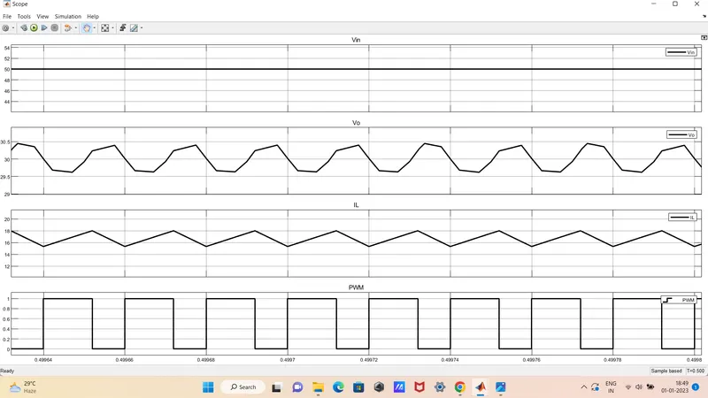
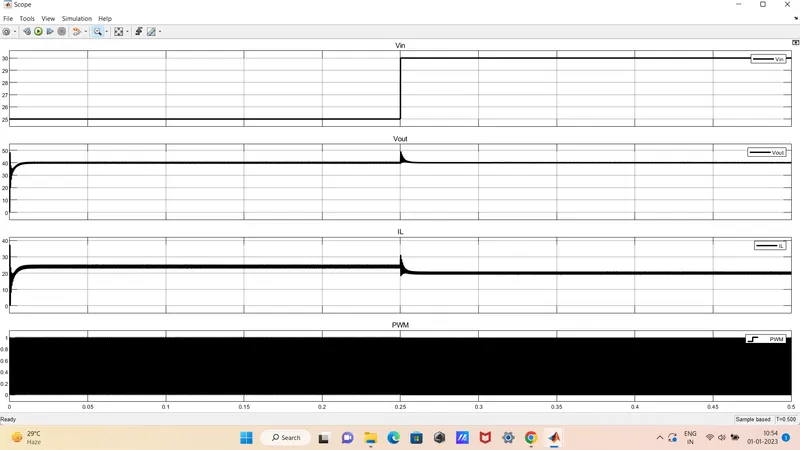
After running the simulation for 0.5 sec, we get the following output waveforms
Zoomed in:
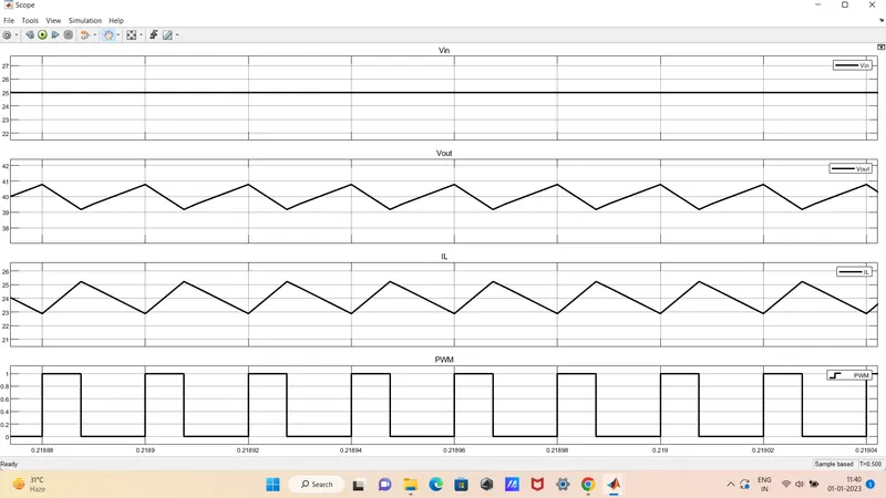
a) Before input disturbance
b) At input disturbance
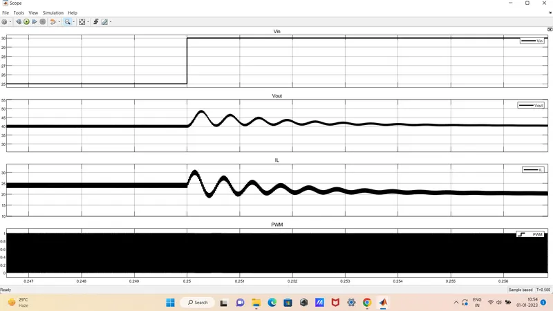
c) After input disturbance
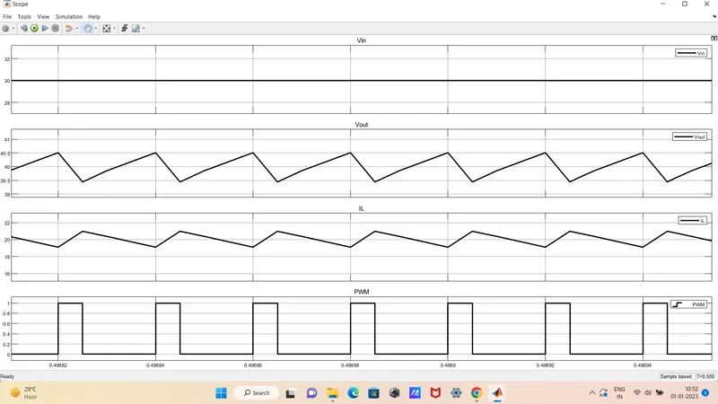
From the above we understood that even though we made a input disturbance at t = 0.25 sec , our system given us the required output. There is small oscillation at the disturbant point but it is less as compared to initial stage. And also we can observe that the inductor current is reduced after the disturbance.
Conclusion:
Thus, the design and simulation of a boost converter is performed and analyized the response.
C) Sepic CCM , Input Voltage 30-60 V , Output Voltage 45 V, Power level 1000W
SEPIC CONVERTER DESIGN AND SIMULATION
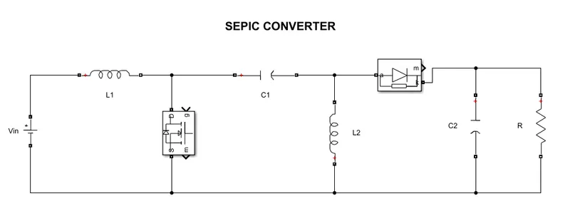
The single-ended primary-inductor converter(SEPIC) is a type of DC/DC converter allowing the electrical potential (voltage) at its output to be greater than, less than, or equal to that at its input. The output of the SEPIC is controlled by the duty cycle. SEPIC converter provides positive regulated output voltage for the given input voltage unlike the buck-boost converter which provides negative regulated output voltage.
The figure below shows the diagram of Sepic converter
Working
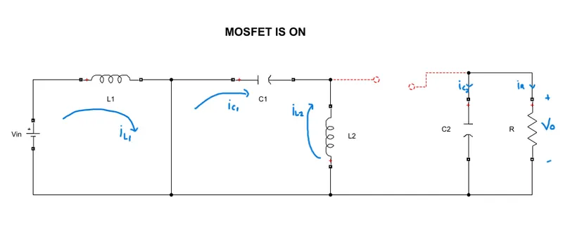
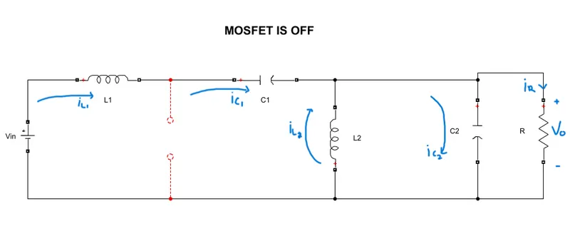
For the SEPIC, when the MOSFET is on, inductor L1 is charged by the input voltage and inductor L2 is charged by capacitor C1. The diode is off and the output is maintained by capacitor C2. When the MOSFET is off, the inductors output through the diode to the load and the capacitors are charged.
The circuit of these modes are given below:
Design
Step 1-Finding the Voltage ratio
The Average inductor voltage is zero, there fore we can write
VL = (von*DT + voff*(1-D)T)/T = 0---------------(1) where D = Duty ratio
by analyzing the voltage waveform of inductor we can write von= Vin and voff = - Vout
substituting the value in equation (1)
.'. Vin*DT + (- Vout)*(1-D)T) = 0
=>Voltage ratio, Vout/Vin = D/(1-D) ------------(2)
Step 2 - Design of converter inductor
Here both inductor are under same exact current and voltage stress, then the ripple current formula for both of them will be the same. However, the inductor current will differ from one inductor to the other.
By analyzing the circuit we can write
IL1 = Iin = Io*(D/(1-D)) = (Vo/R)*(D/(1-D))----(3)
And also IC1 + IL2 = ID = IC2 + Io , average current of capacitor is zero
.'. IL2 = Io------(4)
Design equation of Both inductor is similar
Inductor voltage vL can be written as vL = L*Delta_IL/Delta_t
During ON time , vL = Vin , Delta_t = DT ,
Delta_ILon = Vin*DT/L-----------(5)
During OFF time, vL = - Vout, Delta_t = (1-D)T
Delta_ILoff = (Vout)*(1-D)T)/L-----------(6)
From eq (5) and (6) we can write
L = (Vin*D)/(fs*Delta_IL) = (Vout/fs*Delta_IL)*(1-D)--------(7)
Step 3 - Design of converter Capacitor
Capacitor C2 =>
Capacitance of a capacitor is given C = Q/Vout where Q is charge
=> Delta_Q = C*Delta_Vout--------(8)
Change in charge is the area under the curve for capacitor current
Thus Delta_Q = IR *DT where IR is the output current
=>Delta_Q = (Vout/R)*DT-------(9)
equating (8) and (9)
C2 = D/(R*fs*(Delta_Vout/Vo))-----(10)
Capacitor C1 =>
Capacitance of a capacitor is given C = Q/Vc1 where Q is charge
=> Delta_Q = C*Delta_Vc1--------(11)
Change in charge is the area under the curve for capacitor current
Delta_Q = DT*IL2-------(12) IL2 = Io
equating eq(11) and (12)
C1 = (Vo*D)/(R*fs*(Delta_Vout)------(11)
Components Calculation
Given Vin = 30 - 60 V , Vout = 45 v, Power P = 1kW
assume Vin = 30 v, switching frequency fs = 50kHz
Eq (2) => Duty Ratio = D = Vout/(Vin + Vout)
D = 45/75
D = 0.6
Load Resistance R = Vout^2/P
R = 45^2/1000
R = 2.025 ohm
IL1 = P/Vin = 1000/30
IL1 = 33.33
IL2 = P/Vout = 1000/45
IL2 = 22.22
Let design for 10% ripple in inductor current
Delta_IL1 = 10% of IL1 = 3.33
Delta_IL2 = 10% of IL2 = 2.22
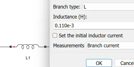
inductance L1min >= (Vin*D)/(fs*Delta_IL1) = 0.108mH
To make sure CCM we choose L1 = 0.11mH
inductance L2min >= (Vin*D)/(fs*Delta_IL1) = 0.162mH
To make sure CCM we choose L2 = 0.17mH
Capacitance C2 = D/(R*fs*(Delta_Vout/Vo))
Let assume output voltage ripple is 5%
=> C = 0.6/(2.025*50000*0.05)
C = 0.118 mF
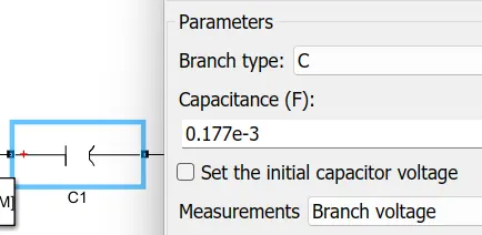
Capacitance C1 = (D*Vo)/(R*fs*(Delta_Vc1))
Let assume voltage ripple is 5%
=> C = (0.6*45)/(2.025*50000*1.5)
C = 0.177 mF
Model
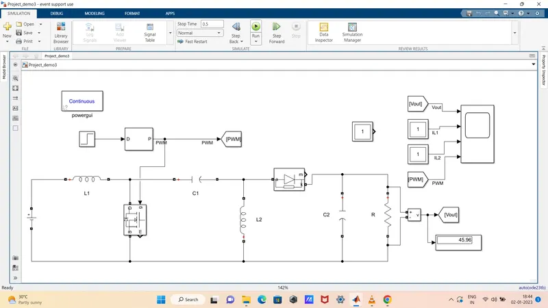
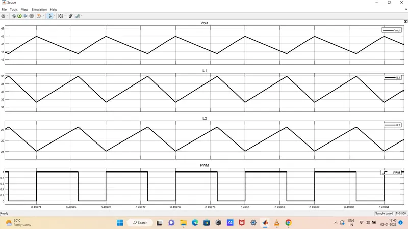
With above information we built a model in simulink and analyzed the response as shown below
Feedback control of Boost converter
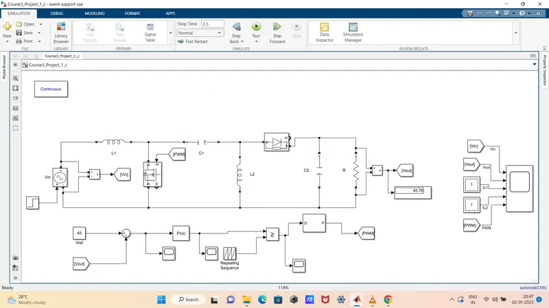
The figure shows the feedback control of Sepic converter.
Here we use PID controller .The controller in this system need to met following requirements
- Output voltage to be acurately regulated
- Output voltage is insensible to disturbance
- Stable feedback system.
- etc..
Using voltage control loop, That is an error signal is made from V_ref and Vout and it is given PI controller. The signal is then compared with a repeating signal to get required switching signal.
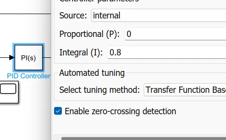
The following are the components and their parameters used to design the above circuit.
1. DC Source Voltage:
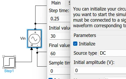
2. Inductor L1
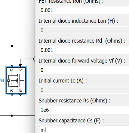
3. MOSFET
4. Capacitor
5. Inductor L2
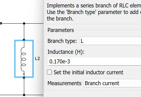
6. Diode
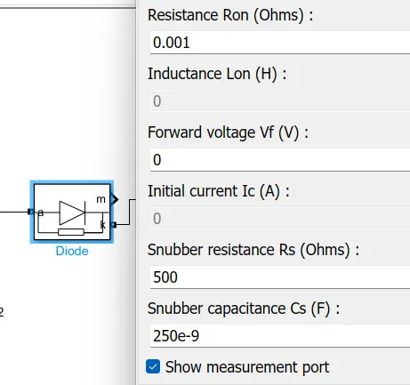
7. Capacitor C2
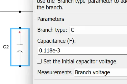
8. Resistor
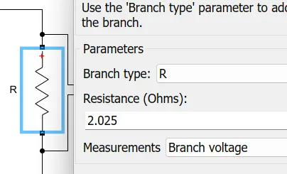
9. Inductor
Result
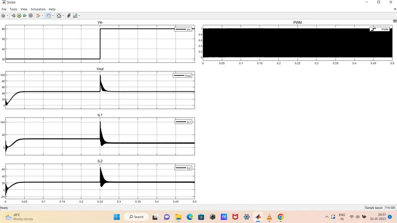
After running the simulation for 0.5 sec, we get the following output waveforms
Here we made a input disturbance at t = 0.25 sec
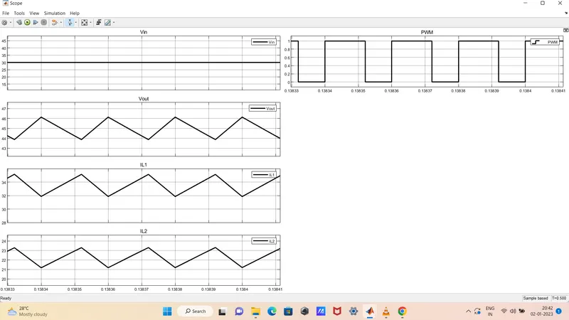
Zoomed in:
a) Before input disturbance
b) At input disturbance
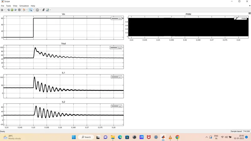
c) After Input disturbance
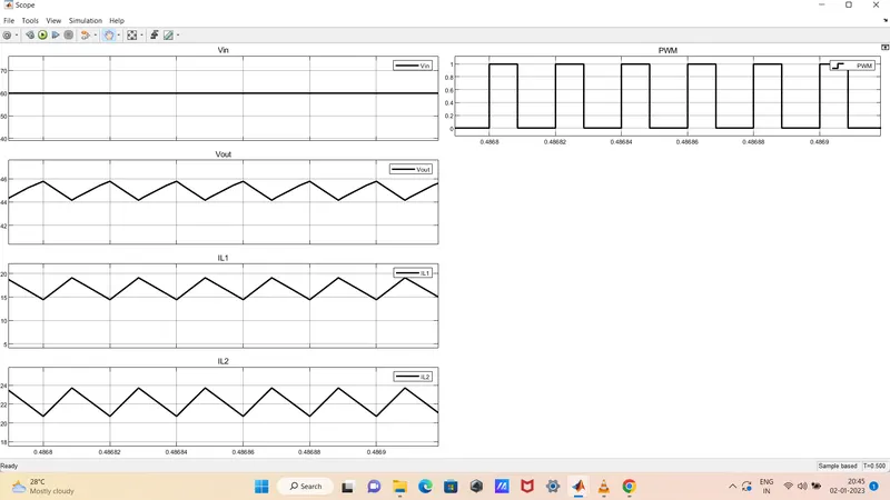
From the above we understood that even though we made a input disturbance at t = 0.25 sec , our system given us the required output voltage but there is a oscillation at the disturbant point.
Conclusion:
Thus, the design and simulation of a boost converter is performed and analyized the response.