Week-7 Challenge: DC Motor Control
AIM:
1. A. Explain a MATLAB demo model named ‘Speed control of a DC motor using BJT H-bridge’.
B. Comment on the armature current shoot-up from the scope results.
C. Refer to the help section of ‘The Four-Quadrant Chopper DC Drive (DC7) block’. Compare it with the H-bridge model.
2. Develop a 2-quadrant chopper using simulink & explain the working of the same with the relevant results. (Refer to article - Multiquadrant operation of motor )
3. Explain in a brief about operation of BLDC motor.
Introduction of Power Switch Devices Used in EV's:
Bipolar Junction Transistor (BJT):
A bipolar junction transistor is a three-terminal semiconductor device that consists of two p-n junctions which can amplify or magnify a signal. It is a current controlled device. The three terminals of the BJT are the base, the collector, and the emitter. A signal of a small amplitude applied to the base is available in the amplified form at the collector of the transistor. This is the amplification provided by the BJT. Note that it does require an external source of DC power supply to carry out the amplification process.
Construction of BJT:
BJT is a semiconductor device that is constructed with 3 doped semiconductor Regions i.e. Base, Collector & Emitter separated by 2 p-n Junctions.
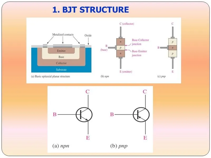
Bipolar transistors are manufactured in two types, PNP and NPN, and are available as separate components, usually in large quantities. The prime use or function of this type of transistor is to amplify current. This makes them useful as switches or amplifiers. They have a wide application in electronic devices like mobile phones, televisions, radio transmitters, and industrial control.
Types of Bipolar Junction Transistor:
There are two types of bipolar junction transistors:
- PNP bipolar junction transistor
- NPN bipolar junction transistor
PNP BJT
In PNP BJT, the n-type semiconductor is sandwiched between the two p-type semiconductors. The two p-type semiconductors act as emitter and collector respectively while the n-type semiconductor acts as a base. This is shown in the figure below.
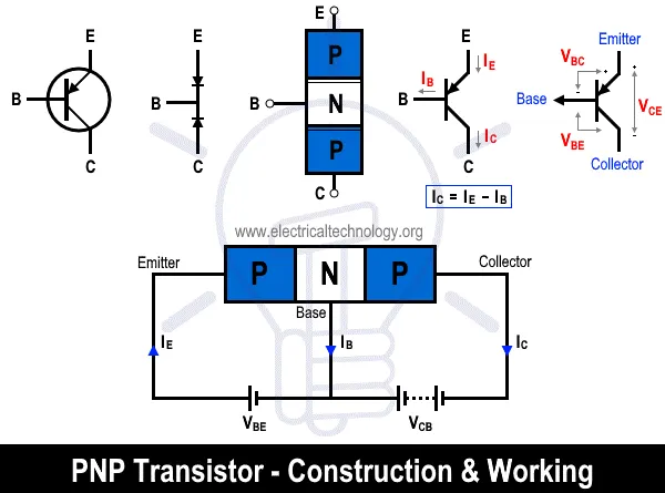
The current enters the transistor through the emitter such that the emitter-base junction is forward biased and the collector-base junction is reverse biased.
NPN BJT:
An NPN BJT, a p-type semiconductor is sandwiched between the two n-type semiconductors. The two n-type semiconductors act as emitter and collector respectively while the p-type semiconductor acts as a base. This is shown in the figure below.
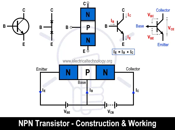
Current entering the emitter, base, and collector has the sign convention of positive while the current that leaves the transistor has the sign convention of negative.
Operation of Bipolar Junction Transistor:
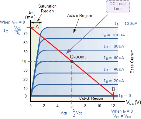
There are three operating regions of a bipolar junction transistor:
- Active region:The region in which the transistors operate as an amplifier.
- Saturation region:The region in which the transistor is fully on and operates as a switch such that collector current is equal to the saturation current.
- Cut-off region:The region in which the transistor is fully off and collector current is equal to zero.
IGBT (Insulated Gate Bipolar Transistor):
IGBT (Insulated Gate Bipolar Transistor) is a three-terminal power switch having high input impedance like P-MOSFET and low on-state power loss as in BJT (Bipolar Junction Transistor. Thus, IGBT is a combined form of the best qualities of both BJT and P-MOSFET. This is the most popular power switch among power-electronics engineers and finds a great variety of applications.
IGBT is a three-terminal device. The three terminals are Gate (G), Emitter (E) and Collector (C). The circuit symbol of IGBT is shown below.
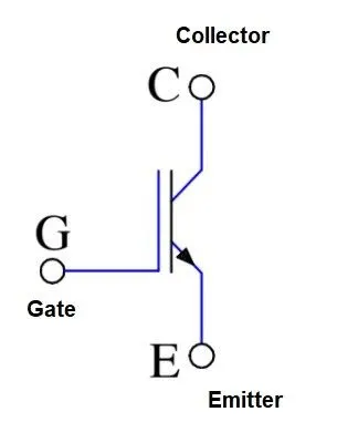
IGBT is also known as metal oxide insulated gate transistor (MOSIGT), conductivity-modulated field-effect transistor (COMFORT) or gain-modulated FET (GEMFET). It was initially called Insulated Gate Transistor (IGT).
Construction of IGBT:
An IGBT is constructed on a p+ layer substrate. On p+ substrate, a high resistivity n-layer is epitaxially grown. As in other semiconductor devices, the thickness of n- layer determines the voltage blocking capability of IGBT. On the other side of the p+ substrate, a metal layer is deposited to form the Collector (C) terminal. Now, p regions are diffused in the epitaxially grown n- layer. Further, n+ regions are diffused in the p region. A basic construction structure of IGBT is shown in the figure below.
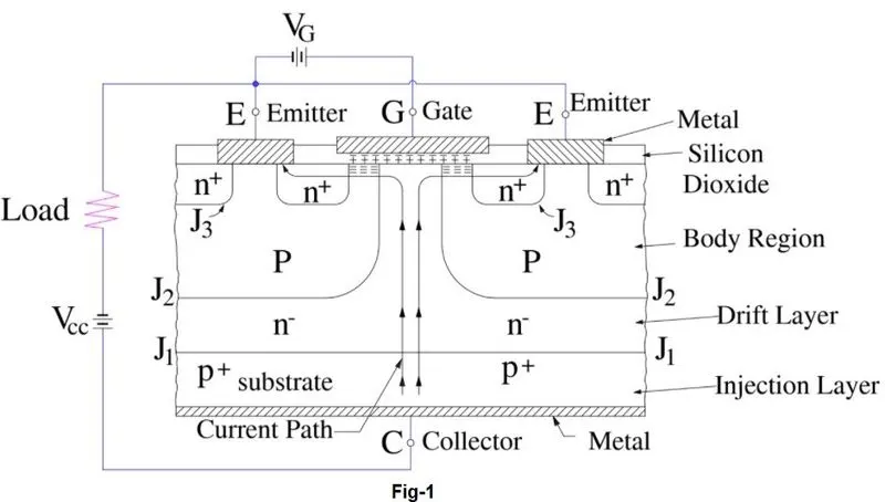
Now, an insulating layer of Silicon Dioxide (SiO2) is grown on the surface. This insulating layer is etched to embed metallic Emitter and Gate terminals.
The p+ substrate is also called the injector layer because it injects holes into n- layer. The n- layer is called the drift region. The next player is called the body of IGBT. The n- layer in between the p+ & p region serves to accommodate the depletion layer of PN- junction i.e. J2.
MOSFET (Metal Oxide Field Effect Transistor):
MOSFET stands for Metal Oxide Field Effect Transistor, MOSFET was invented to overcome the disadvantages present in FETs like high drain resistance, moderate input impedance, and slower operation. So a MOSFET can be called the advanced form of FET. In some cases, MOSFETs are also be called IGFET (Insulated Gate Field Effect Transistor). Practically speaking, MOSFET is a voltage-controlled device, meaning by applying a rated voltage to the gate pin, the MOSFET will start conducting through the Drain and Source pin.
The main difference between FET and MOSFET is that MOSFET has a Metal Oxide Gate electrode electrically insulated from the main semiconductor n-channel or p-channel by a thin layer of Silicon dioxide or glass. The isolation of the controlling Gate increases the input resistance of the MOSFET extremely high in the value of the Mega-ohms (MΩ).
Symbol Of MOSFET:
In general, the MOSFET is a four-terminal device with a Drain (D), Source (S), gate (G) and a Body (B) / Substrate terminals. The body terminal will always be connected to the source terminal hence, the MOSFET will operate as a three-terminal device. In the below image, the symbol of N-Channel MOSFET is shown on the left and the symbol of P-Channel MOSFET is shown on the right.
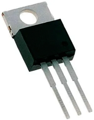
The most commonly used package for MOSFET is To-220, for a better understanding let’s take a look at the pinout of the famous IRF540N MOSFET (shown below). As you can see the Gate, Drain, and Source pins are listed below, do remember that the order of these pins will change based on the manufacturer. The other popular MOSFETs are IRFZ44N, BS170, IRF520, 2N7000, etc
MOSFET as a Switch:
The most common application of a MOSFET is using it as a switch. The below circuit shows the MOSFET operating as a Switching device for turning ON and OFF of the lamp. The gate input voltage VGS applied with the help of an input voltage source. When the applied voltage is positive, the motor will be in the ON state and if the applied voltage is zero or negative, the lamp will be in an OFF state.
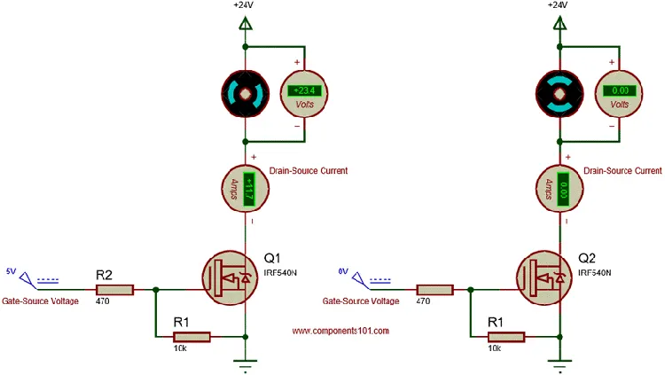
When you turn on a Mosfet by supplying the required voltage to the gate pin, it will remain on unless you supply 0V to the gate. To avoid this problem, we should always use a pull-down resistor (R1), here I have used a value of 10k. In applications like controlling the speed of the motor or dimming light, we would use a PWM signal for fast switching, during this scenario the MOSFET’s gate capacitance will create a reverse current due to the parasitic effect. To tackle this, we should use a current limiting capacitor, I have used a value of 470 here.
Construction Of MOSFET:
The below image shows the typical internal structure of the MOSFET. Although the MOSFET is an advanced form of FET and operates with the same three terminals as a FET the internal structure of the MOSFET is really different from the general FET.
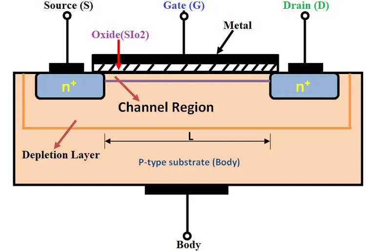
If you look at the structure, you could see that the gate terminal is fixed on the thin metal layer which is insulated by a layer of Silicon Dioxide (SiO2) from the semiconductor, and you will be able to see two N-type semiconductors fixed in the channel region where the drain and source terminals are placed. The channel between the drain and source of the MOSFET is an N-type, opposite to this, the substrate is implemented as P-type. This helps in biasing MOSFET in both the polarities, either positive or negative. If the gate terminal of the MOSFET isn’t biased, it will stay in the non-conductive state, hence the MOSFET is mostly used in designing switches and logic gates.
Working Principle of MOSFET:
In general, the MOSFET works as a switch, the MOSFET controls the voltage and current flow between the source and drain. The working of the MOSFET depends on the MOS capacitor, which is the semiconductor surface below the oxide layers between the source and drain terminal. It can be inverted from p-type to n-type, simply by applying positive or negative gate voltage respectively. The below image shows the block diagram of the MOSFET.
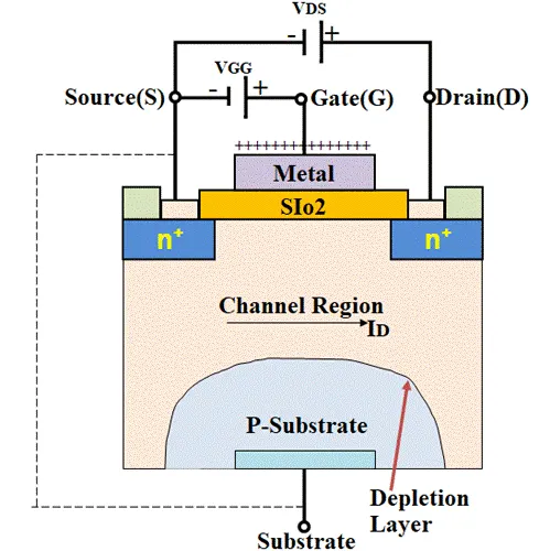
When a drain-source voltage (VDS) is connected between the drain and source, a positive voltage is applied to the Drain, and the negative voltage is applied to the Source. Here the PN junction at the drain is reverse biased and the PN junction at the Source is forward biased. At this stage, there will not be any current flow between the drain and the source.
If we apply a positive voltage (VGG) to the gate terminal, due to electrostatic attraction the minority charge carriers (electrons) in the P substrate will start to accumulate on the gate contact which forms a conductive bridge between the two n+ regions. The number of free electrons accumulated at the gate contact depends on the strength of the positive voltage applied. The higher the applied voltage greater the width of the n-channel formed due to electron accumulation, this eventually increases the conductivity and the drain current (ID) will start to flow between the Source and Drain. When there is no voltage applied to the gate terminal, there will not be any current flow apart from a small amount of current due to minority charge carriers. The minimum voltage at which the MOSFET starts conducting is called the threshold voltage.
Operation of MOSFET in Depletion Mode:
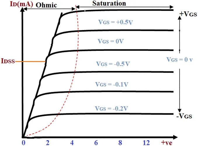
The depletion-mode MOSFETs are usually called the “Switched ON” devices as they are generally in the closed state when there is no bias voltage at the gate terminal. When we increase the applied voltage to the gate positive the channel width will be increased in depletion mode. This will increase the drain current ID through the channel. If the applied gate voltage is highly negative, then the channel width will be less and the MOSFET might enter into the cutoff region.
VI characteristics:
The V-I characteristics of the depletion-mode MOSFET transistor are drawn between the drain-source voltage (VDS) and Drain current (ID). The small amount of voltage at the gate terminal will control the current flow through the channel. The channel formed between the drain and the source will act as a good conductor with zero bias voltage at the gate terminal. The channel width and drain current will increase if the positive voltage is applied to the gate whereas they will get decreased when we apply a negative voltage to the gate.
Operation of MOSFET in Enhancement Mode:
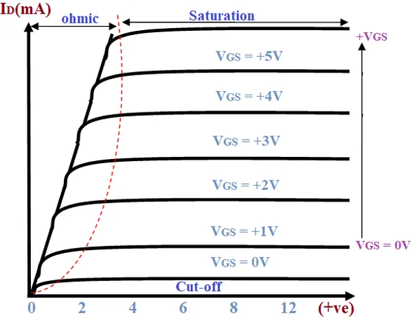
The operation of MOSFET in Enhancement mode is similar to the operation of the open switch, it will start to conduct only if the positive voltage(+VGS) is applied to the gate terminal and the drain current starts to flow through the device. The channel width and drain current will increase when the bias voltage increases. But if the applied bias voltage is zero or negative the transistor will remain in the OFF state itself.
VI Characteristics:
VI characteristics of the enhancement-mode MOSFET are drawn between the drain current (ID) and the drain-source voltage (VDS). The VI characteristics are partitioned into three different regions, namely ohmic, saturation, and cut-off regions. The cutoff region is the region where the MOSFET will be in the OFF state where the applied bias voltage is zero. When the bias voltage is applied, the MOSFET slowly moves towards conduction mode, and the slow increase in conductivity takes place in the ohmic region. Finally, the saturation region is where the positive voltage is applied constantly and the MOSFET will be staying in the conduction state.
Q.1) A. Explain a MATLAB demo model named ‘Speed control of a DC motor using BJT H-bridge’.
ANS:
H-bridge switches:
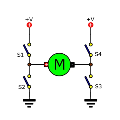
Fig.1: All the switches are OFF, causing the motor to not rotate.
In-circuit, we see that all switches are open states. No the current flowing in the circuit, cause the DC motor can’t work.
Forwarding Mode
Then, look at Fig. 2. When having the S1-switch (closed) and S3 (closed).
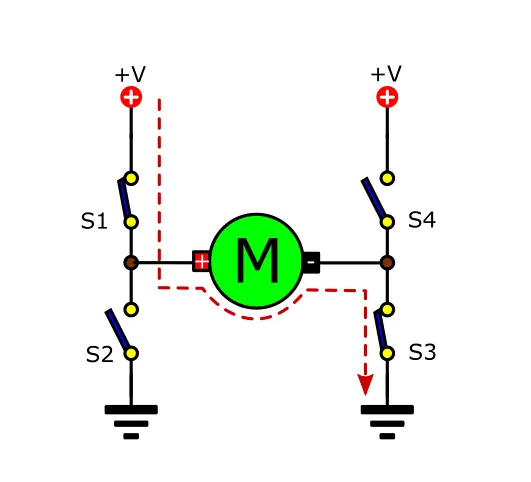
Fig.2: the switch S1 and S3 are closed cause the motor rotates.
It causes the motor to get the current. As we notice that the current flowing into the positive terminal of the motor.
Making the DC motor rotated in features of forwarding form. Or Rotate clockwise.
Reversed Mode
And, If both S4 and S2 are closed together. The Motor also get current that flow through them. But it will don’t be the same first form. As Fig. 3
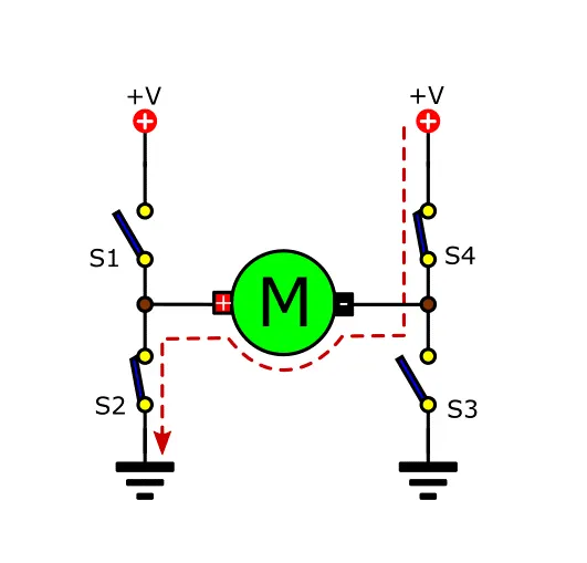
Fig. 3: Both switch-S2 and S4 are closed, causes the DC motor to rotate back in the counter-clockwise direction.
Because that current will flow through the negative of motor cause current reversed or Rotated back counter-clockwise direction.
Start to apply transistors:
We will try to use all the transistors as the switch. You see in Fig. 4.
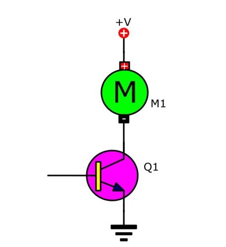
Fig. 4 Using the transistor as switches.
When a base of transistors gets the current electricity. It causes the transistor running and the DC motor will rotate, too.
Bridge transistor Motor driver
As Fig. 5, we use the four transistors to connected to the H-bridge circuit.
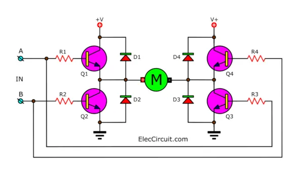
Fig.5: we use the four transistors as a switch controller.
And add a diode to protect the electricity that may flow backwards from the motor. Making damage to the transistor.
Forward Rotate using transistors
In Fig. 6 circuit, if we apply power to A-point. We will make Q1 and Q3-transistor works. Because they get IB-current into a base.
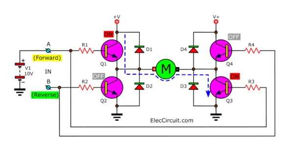
Fig. 6: apply power into A-point, Q1 and Q3 work. The motor rotates forward directions.
So, the motor will rotate in the forward direction. Because the electrical current flowing from Q1 into the positive of the motor. and flow through Q3 to ground successfully.
Reverse Rotate control using transistor:
Then later as in Fig. 7, we change the power supply-V1 point into B-point. The Q4 and Q2 also work by they get current from the base.
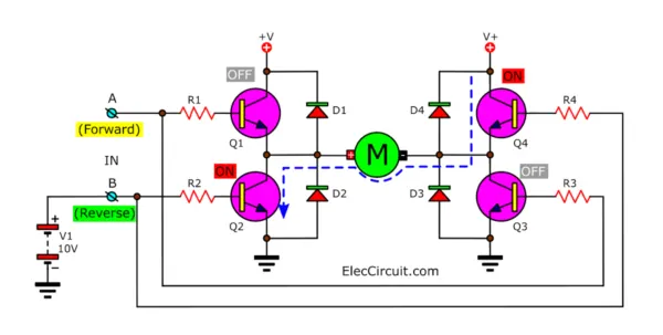
Fig. 7: The motor gets the current through Q4 and Q2. It rotates in the reverse direction
It makes them have the current flow through Q4 go to the negative of motor and through Q2-transistors to ground. Which flowing of current in this form causes the motor to rotate in the reverse direction.
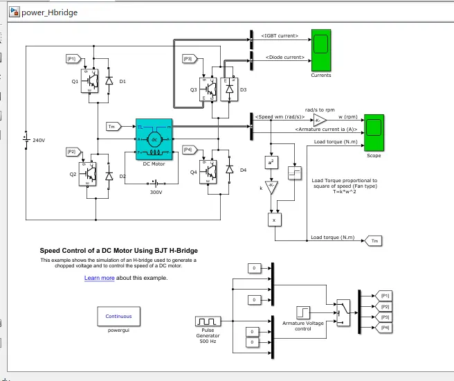
The Bipolar Junction Transistor (BJT) when used for power switching applications, operates as an IGBT. When it is conducting (BJT operating in the saturated region), a forward voltage Vf is developed between collector and emitter (in the range of 1 V). Therefore, the IGBT block can be used to model the BJT device. The IGBT block does not simulate the gate current controlling the BJT or IGBT. The switch is controlled by a Simulink signal (1/0).
Model Description:
- The DC motor uses the preset model (5 HP 24V 1750 rpm). It simulates a fan type load (where Load torque is proportional to the square of speed).
- The armature means voltage can be varied from 0 to 240 V when the duty cycle (specified in the Pulse Generator block) is varied from 0 to 100%.
- The H-bridge consists of four BJT/Diode pairs (BJT simulated by IGBT models). Two transistors are switched simultaneously: Q1 and Q4 or Q2 and Q3. When Q1 and Q4 are fired, a positive voltage is applied to the motor and diodes D2-D3 operate as free-wheeling diodes
- When Q1 and Q4 are switched off. When Q2 and Q3 are fired, a negative voltage is applied to the motor and diodes D1-D4 operate as free-wheeling diodes when Q2 and Q3 are switched off.
- A Switch block at bottom of the circuit Splits the Power Supply into 4 parts namely they are [[p) (p2) [p3) [p4]]. These inputs are in the Goto form block.
- That block is used to send a signal to "From Block" that have the specified tag. If the tag visibility is "scoped, then a Goto tag visibility block must be used to define the visibility of that particular tag. The block icon displays the selected tag name (local tag are enclosed in bracket " and Scoped tag names are enclosed in braces" 0)
- Therefore these 4 types of Input are connected to transistor Ql Q2, Q3, and Q4 through "From Block"; An "From block" Receives. the Signal from the "Goto Block" with the specified tag The block icon displays the selected tag name (local tags are enclosed in [] brackets and Scoped tag names are enclosed in brace{} brackets).
SWITCHES:
Q1 and Q2=Forward Motoring
Q2 and Q3=Reverse Motoring.
- This formation is called an H-Bridge. An H-bridge is an arrangement of transistor that allows a circuit full control over a standard Electric DC Motor
- The DC Motor is connected to the battery and the Mechanical Input of the DC Motor is Initiated as torque.
- Load Torque Proportional to Square of Speed
T=k* ω^2
Where,
T= Load torque
ω = Speed
- Torque for Mechanical input of DC motor also switched by Goto and From
- The Output of the DC motor is connected with the "BUS sector whereas the Speed is plotted in the Scope. A conversion of Speed from rad/sec to rpm is held between the BUS sectors to scope using converter block.
OUTPUT RESULTS:
Q.1) B. Comment on the armature current shoot-up from the scope results.
ANS:
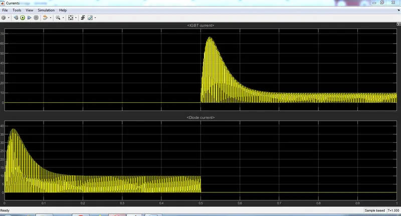
- In the Current output, the amount of circuit acted is shown as the graphical representation during the period of duty cycle. The scope shows IGBT current and Diode current passed in the Quadrant Q3 and D3 (as initial current is in diode to start the circuit is in D3 diode).
- Where Q3 represent IGBT current and D3 is represented as Diode current in scope.
The Graph shows that when the Switch 03 is OFF on the Starting Stage of Current flow and Diode current is on that I stage.
- During the 0.5 sec of time D3 switch is ON that are given. according to Pulse generator (step time in armature voltage control of 0.5) and after the time period of 0.5 sec D3 switch is OFF and IGBT current is acted after 0.5 sec and Q3 switch remains ON.
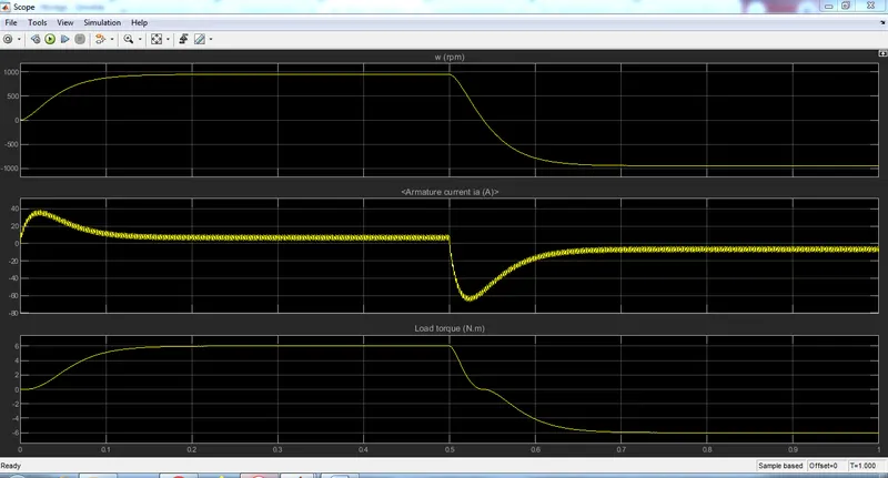
- The Speed and Armature current is obtained by the DC Motor and Load Torque is Calculated by load torque proportional to the square of the speed Starting point, there is a sudden Shoot up is acted.
- In this Scope shows that speed is increased in a certain period of time and at that time armature current is positive whereas Load Torque also moves forward.
- After the time period of 0.5 sec which is given in Pulse generator (step time), sudden shoot-up is acted and speed gets decreased in that time armature current is in negative terminal whereas Torque act as reverse action.
- Here the sudden shoot up is acted while Armature current is processed at a positive and negative terminal
BY CHANGING THE PULSE GENERATOR INPUT (TO VALUE REDUCE THE SHOOT UP OF ARMATURE CURRENT):
- One simple and easy way to control the Speed of a Motor is to Regulate the Amount of Voltage across its Terminals and this can be achieved using "Pulse Width Modulation.
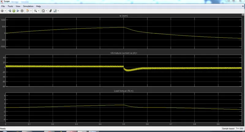
- For Experimental Section we will reduce the Pulse width (Le refer as DUTY CYCLE) of the Pulse generator block by 50% at the same time period.
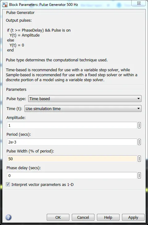
- The Inputs of Pt. P2, P3 and P4 are also changed according to the drive cycle. When the Qland Q4 switch is ON the Motor is generated as a Forwarding direction that state Q3 switch and Q2 the switch is in OFF.
- When the Q2 and Q3 switch is ON the Motor is generated as the reverse direction that state Q1 and Q4 switch is in OFF Condition.
- The change made as 50% of Pulse width are Shown as below.
Q.1) C. Refer to the help section of ‘The Four-Quadrant Chopper DC Drive (DC7) block’. Compare it with the H-bridge model.
ANS:
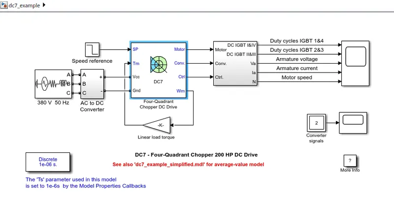
Model Description:
The 200 HP DC motor is separately excited with a constant 150 V DC field voltage source. The armature voltage is provided by an IGBT converter controlled by two PI regulators. The converter is fed by a 515 V DC bus obtained by rectification of a 380 V AC 50 Hz voltage source. To limit the DC bus voltage during dynamic braking mode, a braking chopper has been added between the diode rectifier and the DC7 block.
The first regulator is a speed regulator, followed by a current regulator. The speed regulator outputs the armature current reference (in p.u.) used by the current controller to obtain the electromagnetic torque needed to reach the desired speed. The speed reference change rate follows acceleration and deceleration ramps to avoid sudden reference changes that could cause armature over-current and destabilize the system. The current regulator controls the armature current by computing the appropriate duty ratios of the 5 kHz pulses of the four IGBT devices (Pulse Width Modulation). For proper system behaviour, the instantaneous pulse values of IGBT devices 1 and 4 are opposite to those of IGBT devices 2 and 3. This generates the average armature voltage needed to obtain the desired armature current. To limit the amplitude of the current oscillations, a smoothing inductance is placed in series with the armature circuit.
Working of Four-Quadrant Chopper DC Drive:
Circuit Diagram:
The Four-Quadrant chopper circuit diagram is shown in Fig. 1. Here the motor load is assumed, R and La armature resistance and inductance of the motor respectively. Eb is the back emf of the motor.
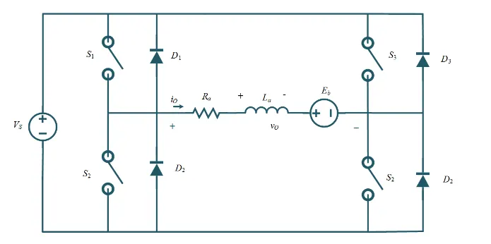
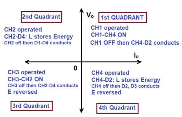
Quadrant I operation when Switch S1 turned on:
The Four-Quadrant chopper equivalent circuit diagram for Quadrant I is shown in Figure 3. Here switch S1, operated, Switches S1, and S4 conduct, output voltage Vo and the output current to both are positives, power flows from source to load and inductor stores energy, the motor rotates in the forward direction hence called forward motoring.
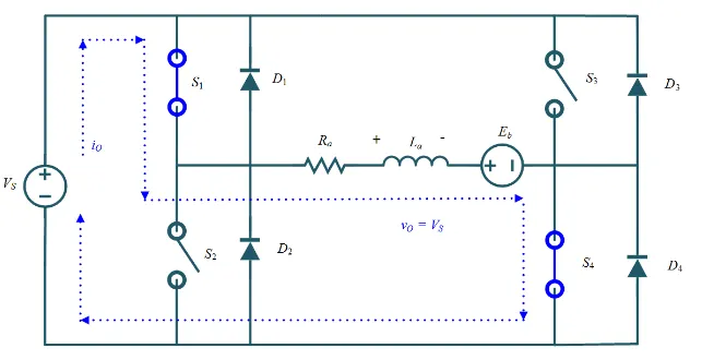
Quadrant I operation when Switch S1, turned off:
The Four-Quadrant chopper equivalent circuit diagram for Quadrant is shown in Figure 4. Switch S1, turned off but switch S4, and diode D2, conducts, the output current is i0 positive and the output voltage Vo becomes zero, inductor release energy and free-wheeling and action using diode D2 takes place, the motor rotates in the forward direction hence called forward motoring.
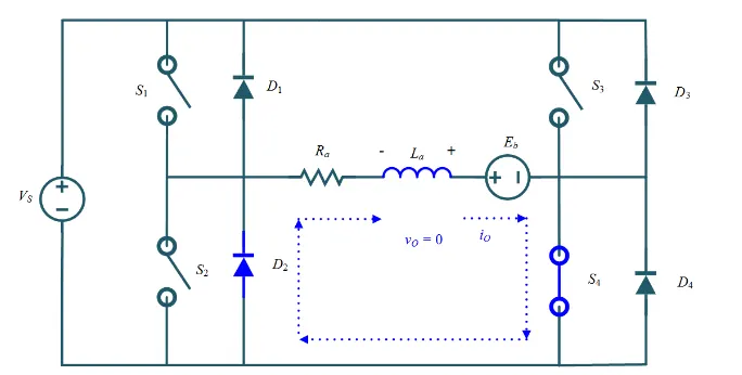
Quadrant II operation when Switch S2, turned on:
The Four-Quadrant chopper equivalent circuit diagram for Quadrant II is shown in Figure 5 Let us assume that the motor is running in the forward direction. Here switch S2, operated Switch S2, and diode D4, conducts, the output voltage Vo is zero and Eb, is responsible for the negative output current (machine behave as gen generator and inductor stores energy).
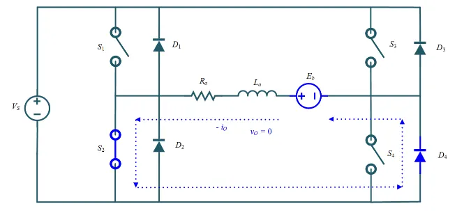
Quadrant II operation when Switch S2, turned off:
The Four-Quadrant chopper equivalent circuit diagram for Quadrant II is shown in Figure 6. Switch S2, turned off, diode D1, and diode D4 conducts, output voltage Vo, becomes positive and the output current Io is negative, inductor release energy using diodes D1 and D4, power flows from load to source and hence called as reverse braking.
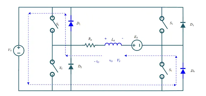
Quadrant III operation when Switch S3, turned on:
The Four-Quadrant chopper equivalent circuit diagram for Quadrant III is shown in Figure 7. The polarity of back emf Eb must be reversed. Here switch S3, operated, Switches S3, and S2, conducts, the output voltage Vo and the output current io both are negatives. Power flows from source to load and the inductor stores the motor rotates in the reverse direction hence called reverse motoring.
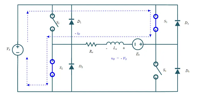
Quadrant III operation when Switch S3, turned off:
The Four-Quadrant chopper equivalent circuit diagram for Quadrant III is shown in Figure 8. The polarity of back emf Eb must be reversed Switch S3, turned off but switch S2, and diode D4 conducts, output current lo is negative and the output voltage Vo becomes zero, inductor release energy and free-wheeling action using diode D4, takes place, the motor rotates in the reverse direction hence called Reverse motoring.
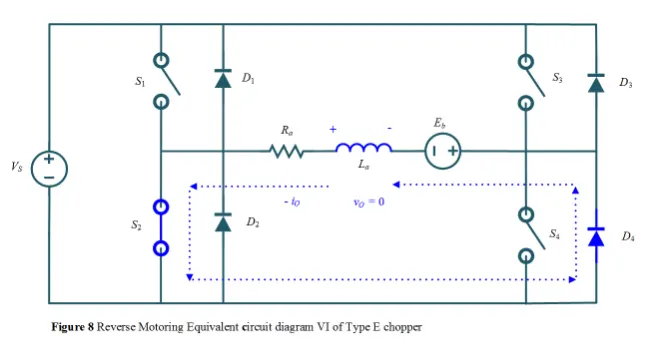
Quadrant IV operation when Switch S4, turned on:
The Four-Quadrant chopper equivalent circuit diagram for Quadrant IV is shown in Figure 9. The polarity of back emf Eb must be reversed. Let us assume that the motor is running in the reverse direction. Here switch S4 operated, Switches S4, and diode D2 conducts, the output voltage Vo is zero and Eb is responsible for the positive output current io machine behave as generator and inductor stores energy.
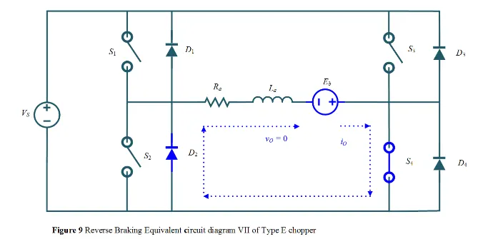
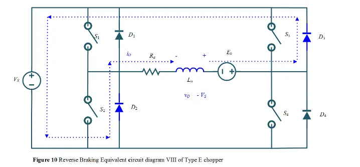
Quadrant IV operation when Switch S4, turned off:
The Four-Quadrant chopper equivalent circuit diagram for Quadrant is shown in Figure 10. The polarity of hack emf Eb must be reversed Switch S4 turned off, diode D2, and diode D3 conducts output voltage Vo becomes negative and output current io positive, inductor release energy using diodes D2, and D3, power flows from load to source and hence called a reverse braking.
COMPARISON OF 4 QUADRANT CHOPPER AND BJT H-BRIDGE:
1) The 4 quadrant chopper works in all four modes like,
- forward motoring
- forward breaking
- reverse motoring
- reverse breaking
And the BJT H- bridge model:
- forward motoring
- reverse motoring
2)To change the direction of rotation of motor from forward to reverse and vice versa, the current signals get transited from one to another switch while in h bridge model, the direction of rotation of the motor is changed by changing the polarity of the current.
3)The 4 quadrant chopper have a high switching frequency while the h bridge model has a low switching frequency
4)The armature current in the 4 quadrant chopper has a little spike at the transition from one to another switch because of high switching frequency while the h bridge model has a high spike of current.
5)The 4 quadrant chopper is generally used in an industrial application while the h bridge model is used in robotics.
Q.2) Develop a 2-quadrant chopper using simulink & explain the working of the same with the relevant results. (Refer to article - Multiquadrant operation of motor )
ANS:
A 2-quadrant Chopper Explanation:
A 2-quadrant Chopper is a category of the chopper that can operate in the first as well as a second quadrant. This basically means that the power can either flow from source to load or load to source in this chopper. This kind of chopper is also known as the Two Quadrant Class-A chopper. In this article, we will discuss A 2-quadrant chopper, its working principle with the help of a circuit diagram and its application.
Operation / Working of A 2-quadrant Chopper:
As we know that, a Class-A and Class-B chopper operates in the first and second quadrants respectively. Therefore, if we connect both these types of the chopper in parallel then it is possible to have chopper operation in the first as well as a second quadrant.
In fact, A 2-quadrant chopper is obtained by the parallel connection of Class-A and Class-B chopper. The fig. below shows the circuit diagram of this type of chopper.
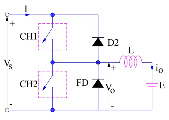
Carefully observe the circuit diagram. You will notice that chopper CH1, free-wheeling diode (FD) and load are forming Class-A Chopper whereas chopper CH2, D2 and Load are forming Class-B chopper. Both these choppers are connected in parallel. To obtain the first quadrant operation we should switch ON chopper CH1 and forgetting the second quadrant operation we should switch ON chopper CH2. Let us discuss this in detail.
Case-1: When CH1 is switched ON / OFF
When chopper CH1 is switched ON, source Vs directly gets connected to the load and hence, load voltage Vo is equal to source voltage. The direction of load current is from source to load as shown in the circuit diagram which is assumed positive.
When CH1 is switched OFF, the free-wheeling diode FD comes into the circuit as it gets forward biased and hence shorts the load. Therefore, the output voltage Vo becomes zero. However, the io continues to die down through the FD and L in the same direction as shown in the circuit diagram. Thus, the average output voltage Vo and current Io are positive and hence the operation of the chopper is in the first quadrant. In fact, this is the Class-B mode of operation.
Case-2: When CH2 is switched ON / OFF
When chopper CH2 is switched ON, load DC source E drives current through CH2 and load. The direction of this current io will be opposite to that shown in the circuit diagram and hence is assumed negative. Output voltage Vo is zero during this time. When CH2 is made OFF, diode D2 gets forward biased and hence the current into the source from the load. The output voltage is Vs in this time as the load is connected to the source through D2 during the OFF time of chopper CH2. Thus, the load current is always negative i.e. operation of the chopper is within the second quadrant. In fact, this is the Class-B mode of operation.
From the above two cases, we can conclude the following points:
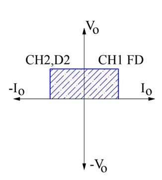
- The output voltage Vois zero when chopper CH2 is ON or free-wheeling diode FD conducts.
- The output voltage Vois equal to source voltage Vs when chopper CH1 is ON or diode D2 conducts.
- The load current flows in the direction shown in the circuit diagram i.e.iois positive when CH1 is ON or FD conducts.
- The load current flows opposite to the direction shown in the circuit diagram i.e.iois negative when CH2 is ON or D2 conducts.
The average load voltage is always positive but the average load current may be positive or negative. Therefore, power flow may be from the source to load (first quadrant operation) or load to the source (second quadrant operation). The operating region of A 2-quadrant chopper is shown below by hatched area.
Precautions:
Choppers CH1 and CH2 should not be ON simultaneously as this would lead to a direct short circuit on the supply lines.
Developing a 2-quadrant chopper using the Simulink model:
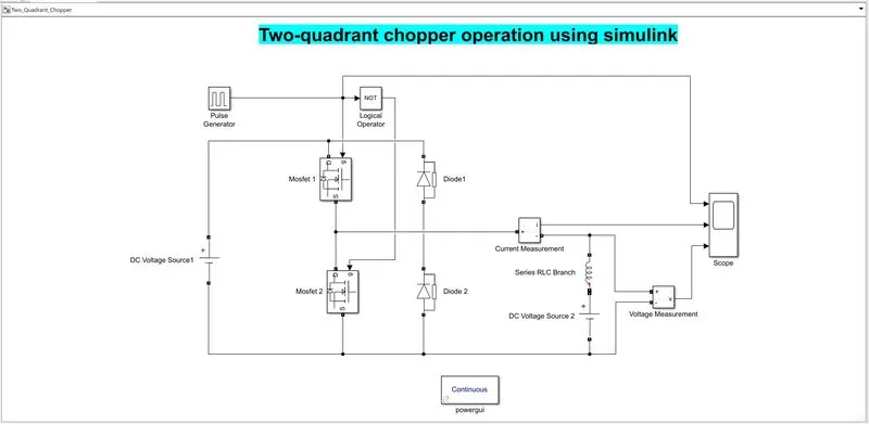
let us take two MOSFET blocks and diodes blocks shown in the circuit diagram.
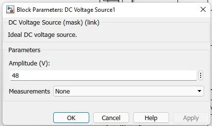
the dc voltage source is connected as shown. let the voltage dc voltage source be 48 volts.
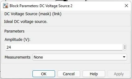
let us consider a series RLC branch block and select inductor L. thus block works as a load to consider LE load le motor load, and de voltage source of 24 volts is also connected in series with an inductor.
The pulse generator block is used to create gate pulse.
The not gate is used in the model so that the two MOSFET will not get closed at the same time otherwise short circuit will occur due to the use of not gate, when one MOSFET is ON the other MOSFET will get off and when another MOSFET is ON the first MOSFET will get off.
The amplitude of pulse generator is kept 12 so that we can clearly see the pulses at the scope and let period be 0.02 seconds and let pulse width be 50%.
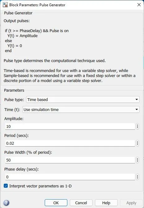
SCOPE RESULT:
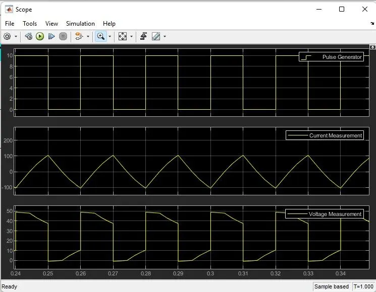
The voltage waveform is not going less than zero the minimum value of voltage is zero and the maximum value is always the positive direction.however, in the current waveform, the current increases and decreases the current may be positive as well as negative and the pulse amplitude is 12 thus from the pulse waveform we can see that the pulse amplitude is 12.
Q.3) Explain in a brief about operation of BLDC motor.
ANS:
Brushless DC motor (BLDC):
A brushless DC motor (known as BLDC) is a permanent magnet synchronous electric motor which is driven by direct current (DC) electricity and it accomplishes an electronically controlled commutation system (commutation is the process of producing rotational torque in the motor by changing phase currents through it at appropriate times) instead of a mechanical commutation system. BLDC motors are also referred to as trapezoidal permanent magnet motors.
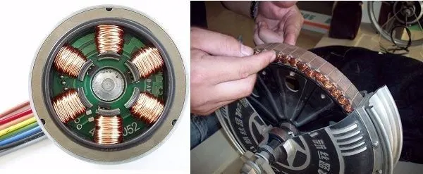
Unlike conventional brushed type DC motor, wherein the brushes make the mechanical contact with a commutator on the rotor to form an electric path between a DC electric source and rotor armature windings, BLDC motor employs electrical commutation with a permanent magnet rotor and a stator with a sequence of coils. In this motor, permanent magnet (or field poles) rotates and current-carrying conductors are fixed.
The armature coils are switched electronically by transistors or silicon controlled rectifiers at the correct rotor position in such a way that the armature field is in space quadrature with the rotor field poles. Hence the force acting on the rotor causes it to rotate. Hall sensors or rotary encoders are most commonly used to sense the position of the rotor and are positioned around the stator. The rotor position feedback from the sensor helps to determine when to switch the armature current.
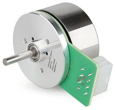
This electronic commutation arrangement eliminates the commutator arrangement and brushes in a DC motor and hence more reliable and less noisy operation is achieved. Due to the absence of brushes BLDC motors are capable to run at high speeds. The efficiency of BLDC motors is typically 85 to 90 per cent, whereas brushed type DC motors are 75 to 80 per cent efficient. There are wide varieties of BLDC motors available ranging from small power range to fractional horsepower, integral horsepower and large power ranges.
Construction of Brushless DC motor:
In this motor, the permanent magnets are attached to the rotor. The current-carrying conductors are located on the stator. They use electrical commutation to convert electrical energy into mechanical energy.
The main design difference between brushed and brushless motors is the replacement of a mechanical commutator with an electric switch circuit. A BLDC Motor is a type of synchronous motor in the sense that the magnetic field generated by the stator and the rotor revolve at the same frequency.
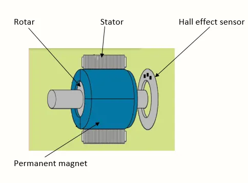
The Brushless motor does not have any current-carrying commutator The field inside a brushless motor is switched through an amplifier which is triggered by the commutating device like an optical encoder.
The layout of a DC brushless motor can vary depending on whether it is in “Outrunner” style or “Inrunner” style.
- Outrunner –The field magnet is a drum rotor that rotates around the stator. This style is preferred for applications that require high torque and where high rpm isn’t a requirement.
- In runner –The stator is a fixed drum in which the field magnet rotates. This motor is known for producing less torque than the outrunner style but is capable of spinning at very high rpm.
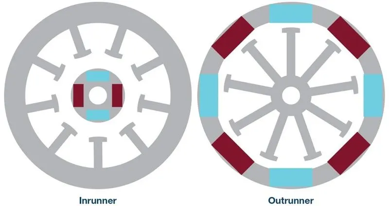
BLDC motors can be constructed in different physical configurations. Depending on the stator windings, these can be configured as single-phase, two-phase, or three-phase motors. However, three-phase BLDC motors with permanent magnet rotors are most commonly used.
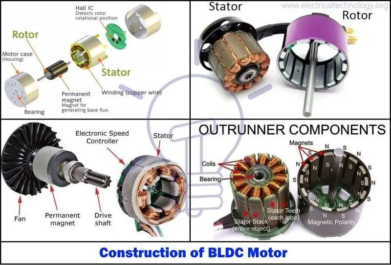
The construction of this motor has many similarities to the three-phase induction motor as well as the conventional DC motor. This motor has stator and rotor parts as like all other motors.
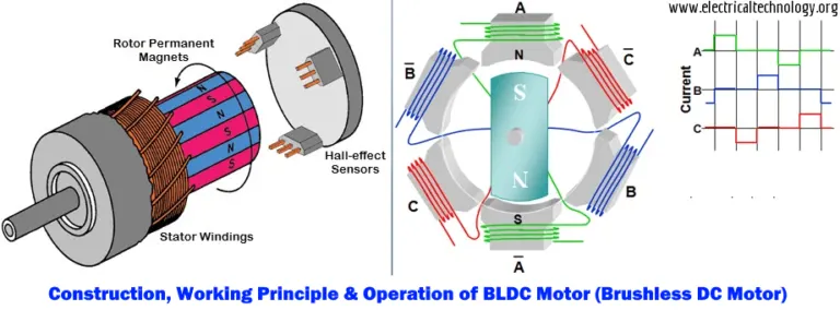
The stator of a BLDC motor is made up of stacked steel laminations to carry the windings. These windings are placed in slots that are axially cut along the inner periphery of the stator. These windings can be arranged in either star or delta. However, most BLDC motors have a three-phase star connected stator.
Each winding is constructed with numerous interconnected coils, where one or more coils are placed in each slot. To form an even number of poles, each of these windings is distributed over the stator periphery.
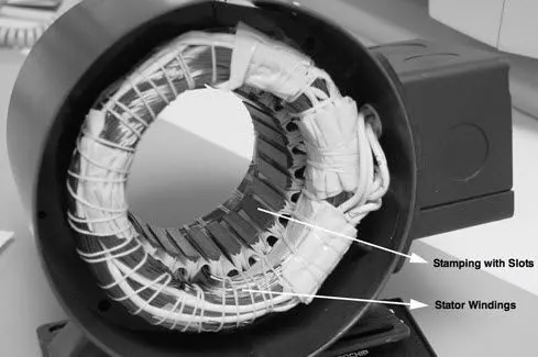
The stator must be chosen with the correct rating of the voltage depending on the power supply capability. For robotics, automotive and small actuating applications, 48 V or less voltage BLDC motors are preferred. For industrial applications and automation systems,100 V or higher rating motors are used.
Rotor:
BLDC motor incorporates a permanent magnet in the rotor. The number of poles in the rotor can vary from 2 to 8 pole pairs with alternate south and north poles depending on the application requirement. To achieve maximum torque in the motor, the flux density of the material should be high. A proper magnetic material for the rotor is needed to produce the required magnetic field density.
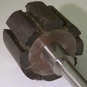
Ferrite magnets are inexpensive, however, they have a low flux density for a given volume. Rare earth alloy magnets are commonly used for new designs. Some of these alloys are Samarium Cobalt (SmCo), Neodymium (Nd), and Ferrite and Boron (NdFeB). The rotor can be constructed with different core configurations such as the circular core with a permanent magnet on the periphery, circular core with rectangular magnets, etc.
Hall Sensors:
Hall sensor provides the information to synchronize stator armature excitation with rotor position. Since the commutation of the BLDC motor is controlled electronically, the stator windings should be energized in sequence to rotate the motor. Before energizing a particular stator winding, acknowledgement of the rotor position is necessary. So the Hall Effect sensor embedded in the stator senses the rotor position.
Most BLDC motors incorporate three Hall sensors which are embedded into the stator. Each sensor generates Low and High signals whenever the rotor poles pass near to it. The exact commutation sequence to the stator winding can be determined based on the combination of these three sensor’s responses.
Working Principle and Operation of BLDC Motor:
BLDC motor works on the principle similar to that of a conventional DC motor, i.e., the Lorentz force law which states that whenever a current-carrying conductor is placed in a magnetic field it experiences a force. As a consequence of the reaction force, the magnet will experience an equal and opposite force. In the case of, BLDC motor, the current-carrying conductor is stationary while the permanent magnet moves.
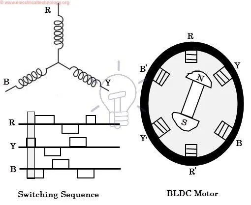
When the stator coils are electrically switched by a supply source, it becomes an electromagnet and starts producing the uniform field in the air gap. Though the source of supply is DC, switching makes to generate an AC voltage waveform with a trapezoidal shape.
Due to the force of interaction between the electromagnet stator and the permanent magnet rotor.
Consider the figure below in which the motor stator is excited based on different switching states. With the switching of windings as High and Low signals, corresponding winding energized as North and South poles. The permanent magnet rotor with North and South poles align with stator poles causing the motor to rotate.
Observe that the motor produces torque because of the development of attraction forces (when North-South or South-North alignment) and repulsion forces (when North-North or South-South alignment). In this way motor moves in a clockwise direction.
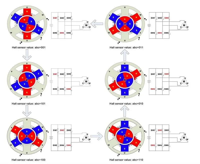
Here, one might get a question that how we know which stator coil should be energized and when to do. This is because; the motor continuous rotation depends on the switching sequence around the coils. As discussed above that Hall sensors give shaft position feedback to the electronic controller unit.
Based on this signal from the sensor, the controller decides particular coils to energize. Hall-effect sensors generate Low and High-level signals whenever rotor poles pass near to it. These signals determine the position of the shaft.
Brushless DC Motor Drive:
As described above that the electronic controller circuit energizes appropriate motor winding by turning transistors or other solid-state switches to rotate the motor continuously. The figure below shows the simple BLDC motor drive circuit which consists of a MOSFET bridge (also called an inverter bridge), electronic controller, hall effect sensor and BLDC motor.
Here, Hall-effect sensors are used for position and speed feedback. The electronic controller can be a microcontroller unit or microprocessor or DSP processor or FPGA unit or any other controller. This controller receives these signals, processes them and sends the control signals to the MOSFET driver circuit.
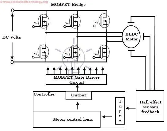
In addition to the switching for a rated speed of the motor, additional electronic circuitry changes the motor speed based on the required application. These speed control units are generally implemented with PID controllers to have precise control. It is also possible to produce four-quadrant operation from the motor whilst maintaining good efficiency throughout the speed variations using modern drives.
Advantages of Brushless DC motor:
- Less overall maintenance due to absence of brushes
- Reduced size with far superior thermal characteristics
- Higher speed range and lower electric noise generation.
- It has no mechanical commutator and associated problems
- High efficiency and high output power to size ratio due to the use of permanent magnet rotor
- High speed of operation even in loaded and unloaded conditions due to the absence of brushes that limits the speed
- Smaller motor geometry and lighter in weight than both brushed type DC and induction AC motors.
- Long-life as no inspection and maintenance is required for commutator system
- Higher dynamic response due to low inertia and carrying windings in the stator
- Less electromagnetic interference
- Low noise due to absence of brushes
Limitations of Brushless DC motor:
- These motors are costly
- The electronic controller required to control this motor is expensive
- Requires complex drive circuitry
- Need of additional sensors
Applications of Brushless DC motor:
Brushless DC motors (BLDC) use for a wide variety of application requirements such as varying loads, constant loads and positioning applications in the fields of industrial control, automotive, aviation, automation systems, health care equipment etc.
- Computer hard drives and DVD/CD players
- Electric vehicles, hybrid vehicles, and electric bicycles
- Industrial robots, CNC machine tools, and simple belt-driven systems
- Washing machines, compressors and dryers
- Fans, pumps and blowers
Reference :
https://www.eleccircuit.com/basic-h-bridge-motor-driver-by-bipolar-transistor/