Week-6 Challenge: EV Drivetrain
AIM:-
- Which types of power converter circuits are employed in electric and hybrid electric vehicles?
- An Electric Vehicle's powertrain with a 72V battery pack is shown in the diagram below. The duty ratio for acceleration operation is 'd1' and for the braking operation the duty ratio is 'd2'.
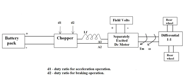
The other parameters of the electric vehicle is given below,
Motor and Controller Parameters:
Rated Armature voltage= 72 V
Rated armature current= 400 A
Ra= 0.5Ω, KΦ= 0.7 Volt second
Chopper Switching frequency= 400 Hz
The vehicle speed-torque characteristics are given by the below equation

What is EV steady-state speed if the duty cycle is 70%?
- Develop a mathematical model of a DC Motor for the below equation using Simulink.
ωω= V/Kϕϕ -Ra/Kϕϕ^2 .T
- Refer to the blog on the below topic:
Induction Versus DC brushless motors by Wally Rippel, Tesla
Explain in brief the author’s perspective.
Question 1
Which types of power converter circuits are employed in electric and hybrid electric vehicles?
THEORY:
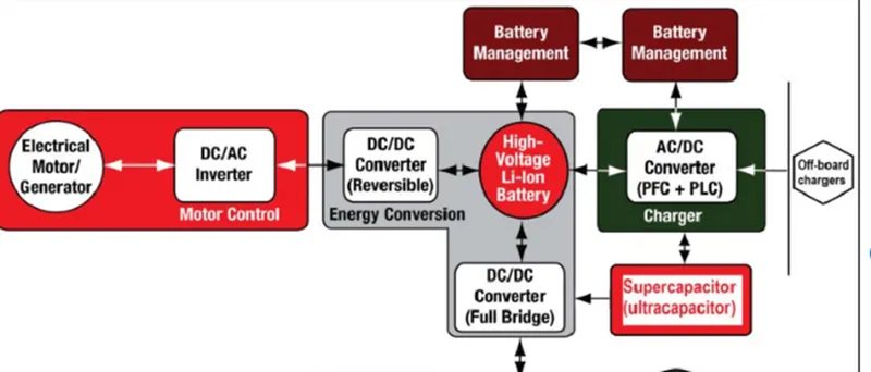
An Electric Vehicle is a vehicle that uses a combination of different energy sources, Fuel Cells (FCs), Batteries and Supercapacitors (SCs) to power an electric drive system as shown in fig 1. In EV the main energy source is assisted by one or more energy storage devices. Thereby the system cost, mass, and volume can be decreased, and a significantly better performance can be obtained. Two often-used energy storage devices are batteries and SCS. They can be connected to the fuel cell stack in many ways. A simple configuration is to directly connect two devices in parallel, (FC/battery, FC/SC, or battery/SC). However, in this way, the power drawn from each device cannot be controlled but is passively determined by the impedance of the devices. The impedance depends on many parameters, e.g. temperature, state-of-charge, health, and point of operation. Each device might therefore be operated in an inappropriate condition, e.g. health and efficiency. The voltage characteristics also have to match perfectly of the two devices, and only a fraction of the range of operation of the devices can be utilized, e.g. in a fuel cell battery configuration the fuel cell must provide almost the same power all the time due to the fixed voltage of the battery, and in a battery/supercapacitor configuration only a fraction of the energy exchange capability of the supercapacitor can be used. This is again due to the nearly constant voltage of the battery. By introducing DC/DC converters one can choose the voltage variation of the devices and the power of each device can be controlled.
Figure 1. Electric vehicle drive system.
In reference, 10 cases of combining the fuel cell with the battery, SCs, or both are investigated. The system volume, mass, efficiency, and battery lifetime were compared. It is concluded that when SCs are the only energy storage device the system becomes too big and heavy. A fuel cell/battery/supercapacitors hybrid provides the longest lifetime of the batteries. It can be noticed that the use of high power DC/DC converters is necessary for EV power supply systems. The power of the DC/DC converter depends on the characteristics of the vehicle such as top speed, acceleration time from 0 to 100 Km/h, weight, maximum torque, and power profile (peak power, continuous power). Generally, for passenger cars, the power of the converter is more than 20 KW and it can go up to 100 KW.
- AC TO DC CONVERTER
- DC TO DC CONVERTER
- DC TO AC CONVERTER
- AC TO DC CONVERTER
AC to DC Converters are one of the most important in power electronics because there are a lot of real applications are based on these conversions. The AC current to dc current conversion process is known as rectification. This rectifier converts the AC supply into the DC supply at the load end connection. Normally Transformers are used to adjust the AC source to get a step-down transformer to reduce the voltage level to have a better operation range for DC supply. Normally this AC to DC converter converts low voltage values.
Uncontrolled converter converts fixed DC voltage, which means the value of output for a given value of AC voltage. A fully controlled converter convert adjustable DC voltage when the adjustable range can adjust in both the positive and negative sides. Semi-controlled converter also produce an adjustable DC voltage which positive side power.
All three converters have unidirectional power flow from the AC side to the DC side. PWN converter can produce adjustable both positive importantly it allows power flow in either direction. Making it ideal application motor drives and power system interconnection with the power system.
All three converters have unidirectional power flow from the AC side to the DC side. PWN converter can produce adjustable both positive importantly it allows power flow in either direction. Uncontrolled rectifiers can also subdivide into several subcategories such as
- Single phase half-wave rectifier.
- Single-phase full-wave bridge rectifier
- Single-phase centre tapped full wave
- Three phases half-wave diode rectifier
a). Single-phase half-wave rectifier:-
Single-phase half-wave rectifier simplest controlled rectifier uses for single devices. To produce variable de voltage from fixed current thyristors are used. Following are the circuit arrangement of the Single-phase half-wave rectifiers. In here diode or thyristors are used. Where the application needs to fix dc Voltage, the diode is used as a switching element. When the application needs variable voltage thyristors are used.
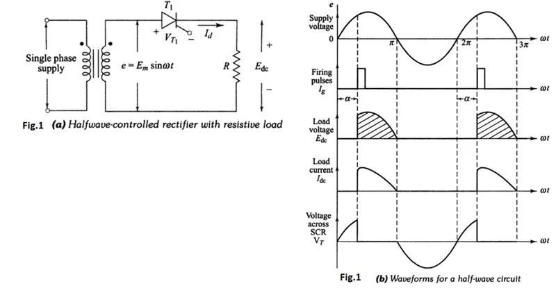
Single-phase converters can mainly classify as Bridge Converter and Center Tapped Converter. This type of uncontrolled converter is mainly used for building supply only in Patrice. In power supply by applying a capacitor filter on the output in other cases which inductive load causes we use this directly or inductive filters.
b). Single-phase full-wave bridge rectifier:-
Another type of circuit that produces the same output waveform as the full-wave rectifier circuit above, is that of the Full Wave Bridge Rectifier. This type of single-phase rectifier uses four individual rectifying diodes connected in a closed-loop “bridge” configuration to produce the desired output.
The main advantage of this bridge circuit is that it does not require a special centre tapped transformer, thereby reducing its size and cost. The single secondary winding is connected to one side of the diode bridge network and the load to the other side as shown below.
The Diode Bridge Rectifier
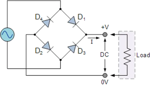
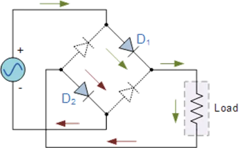
The four diodes labelled D1 to D4 are arranged in “series pairs” with only two diodes conducting current during each half cycle. During the positive half cycle of the supply, diodes D1 and D2 conduct in series while diodes D3 and D4 are reverse biased and the current flows through the load as shown below.
The Positive Half-cycle
During the negative half cycle of the supply, diodes D3 and D4 conduct in series, but diodes D1 and D2 switch “OFF” as they are now reverse biased. The current flowing through the load is in the same direction as before.
The Negative Half-cycle
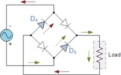
As the current flowing through the load is unidirectional, so the voltage developed across the load is also unidirectional the same as for the previous two diodes full-wave rectifier, therefore the average DC voltage across the load is 0.637Vmax. However in reality, during each half-cycle, the current flows through two diodes instead of just one so the amplitude of the output voltage is two voltage drops ( 2*0.7 = 1.4V ) less than the input VMAX amplitude. The ripple frequency is now twice the supply frequency (e.g. 100Hz for a 50Hz supply or 120Hz for a 60Hz supply.)
Although we can use four individual power diodes to make a full-wave bridge rectifier, pre-made bridge rectifier components are available “off-the-shelf” in a range of different voltage and current sizes that can be soldered directly into a PCB circuit board or be connected by spade connectors.
The image to the right shows a typical single-phase bridge rectifier with one corner cut off. This cut-off corner indicates that the terminal nearest to the corner is the positive or +ve output terminal or lead with the opposite (diagonal) lead being the negative or -ve output lead. The other two connecting leads are for the input alternating voltage from a transformer secondary winding.
c). Single-phase centre tapped full-wave diode rectifier:-
We have already discussed the Full Wave Bridge Rectifier, which uses four diodes, arranged as a bridge, to convert the input alternating current (AC) in both half-cycles to direct current (DC). In the case of a centre-tap full-wave rectifier, only two diodes are used and are connected to the opposite ends of a centre-tapped secondary transformer as shown in the figure below. The centre tap is usually considered as the ground point or the zero voltage reference point.
Working of Centre-Tap Full Wave Rectifier
As shown in the figure, an ac input is applied to the primary coils of the transformer. This input makes the secondary ends P1 and P2 become positive and negative alternately. For the positive half of the ac signal, the secondary point D1 is positive, the GND point will have zero volts and the P2 will be negative. At this instant diode, D1 will be forward biased and diode D2 will be reverse biased. As explained in the Theory Behind P-N Junction and Characteristics of P-N Junction Diode, the diode D1 will conduct and D2 will not conduct during the positive half cycle. Thus the current flow will be in the direction P1-D1-C-A-B-GND. Thus, the positive half cycle appears across the load resistance RLOAD. During the negative half-cycle, the secondary ends P1 becomes negative and P2 becomes positive. At this instant, the diode D1 will be negative and D2 will be positive with the zero reference point being the ground, GND. Thus, the diode D2 will be forward biased and D1 will be reverse biased. The diode D2 will conduct and D1 will not conduct during the negative half cycle. The current flow will be in the direction P2-D2-C-A-B-GND.
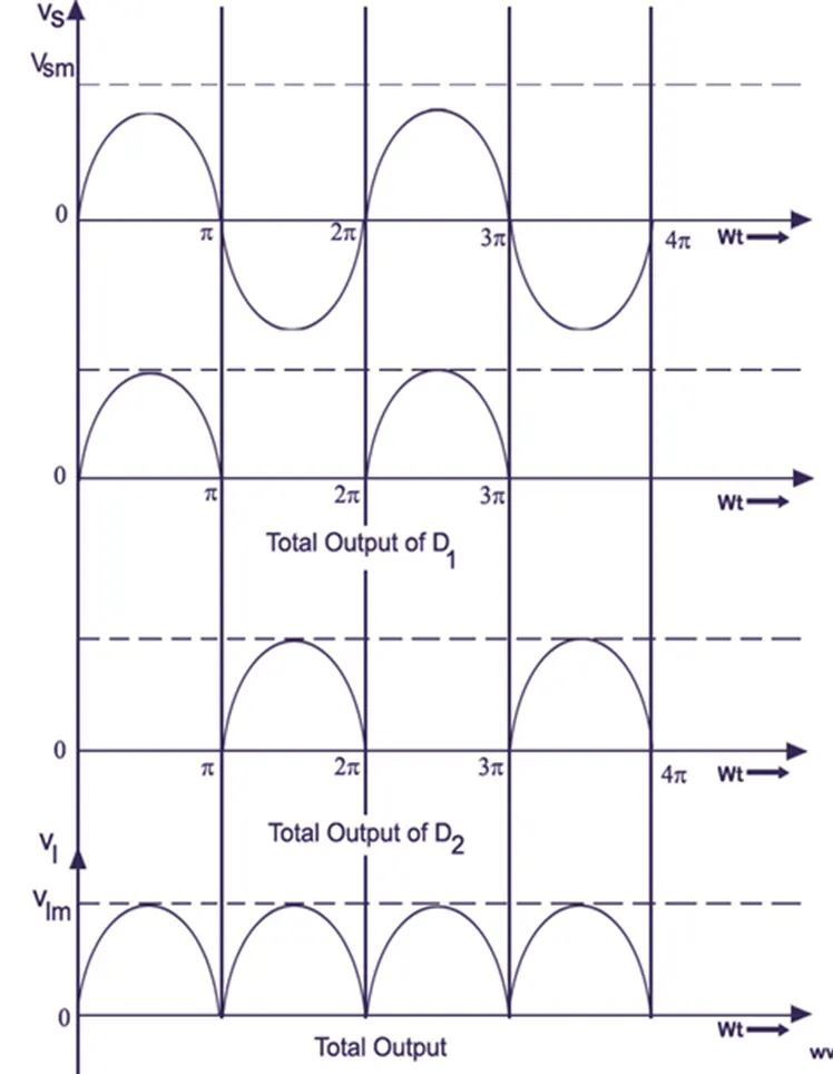
When comparing the current flow in the positive and negative half-cycles, we can conclude that the direction of the current flow is the same (through load resistance RLOAD). When compared to the Half-Wave Rectifier, both the half cycles are used to produce the corresponding output. The frequency of the rectified output voltage is twice the input frequency. The output that is rectified, consists of a dc component and a lot of ac components of minute amplitudes.
d). Three-phase half-wave diode rectifier:-
Three-phase Waveform
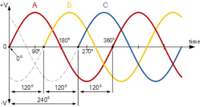
The advantage here is that a three-phase alternating current (AC) supply can be used to provide electrical power directly to balanced loads and rectifiers. Since a 3-phase supply has a fixed voltage and frequency it can be used by a rectification circuit to produce a fixed voltage DC power which can then be filtered resulting in an output DC voltage with less ripple compared to a single-phase rectifying circuit.
Three-phase Rectification
Having seen that a 3-phase supply is just simply three single-phases combined together, we can use this multi-phase property to create 3-phase rectifier circuits.
As with single-phase rectification, three-phase rectification uses diodes, thyristors, transistors, or converters to create half-wave, full-wave, uncontrolled and fully-controlled rectifier circuits transforming a given three-phase supply into a constant DC output level. In most applications, a three-phase rectifier is supplied directly from the mains utility power grid or from a three-phase transformer if a different DC output level is required by the connected load.
As with the previous single-phase rectifier, the most basic three-phase rectifier circuit is that of an uncontrolled half-wave rectifier circuit which uses three semiconductor diodes, one diode per phase as shown.
Half-wave Three-phase Rectification
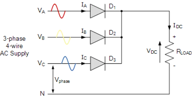
So how does this three-phase half-wave rectifier circuit work? The anode of each diode is connected to one phase of the voltage supply with the cathodes of all three diodes connected together to the same positive point, effectively creating a diode-“OR” type arrangement. This common point becomes the positive (+) terminal for the load while the negative (-) terminal of the load is connected to the neutral (N) of the supply.
Assuming a phase rotation of Red-Yellow-Blue (VA – VB – VC) and the red phase (VA) starts at 0o. The first diode to conduct will be diode 1 (D1) as it will have a more positive voltage at its anode than diodes D2 or D3. Thus diode D1 conducts for the positive half-cycle of VA while D2 and D3 are in their reverse-biased state. The neutral wire provides a return path for the load current back to the supply.
120 electrical degrees later, diode 2 (D2) starts to conduct for the positive half-cycle of VB (yellow phase). Now its anode becomes more positive than diodes D1 and D3 which are both “Of” because they are reversed-biased. Similarly, 120o later VC (blue phase) starts to increase turning “ON” diode 3 (D3) as its anode becomes more positive, thus turning “OFF” diodes D1 and D2.
Then we can see that for three-phase rectification, whichever diode has a more positive voltage at its anode compared to the other two diodes it will automatically start to conduct, thereby giving a conduction pattern of D1 D2 D3 as shown.
Half-wave Three-phase Rectifier Conduction Waveform
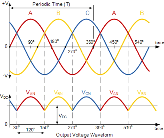
From the above waveforms for a resistive load, we can see that for a half-wave rectifier each diode passes current for one-third of each cycle, with the output waveform being three times the input frequency of the AC supply. Therefore there are three voltage peaks in a given cycle, so by increasing the number of phases from a single-phase to a three-phase supply, the rectification of the supply is improved, that is the output DC voltage is smoother.
For a three-phase half-wave rectifier, the supply voltages VA VB and VC are balanced but with a phase difference of 120o giving:
VA = VP*sin(ωt – 0o)
VB = VP*sin(ωt – 120o)
VC = VP*sin(ωt – 240o)
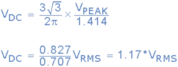
Thus the average DC value of the output voltage waveform from a 3-phase half-wave rectifier is given as:

As the voltage supplies peak voltage, VP is equal to VRMS*1.414, it follows that VP is equal to VP/1.414 giving 0.707*VP, so the average DC output voltage of the rectifier can be expressed in terms of the RMS (root-mean-squared) phase voltage giving:
- DC TO DC CONVERTER
DC-DC converters in an electric vehicle may be classified into unidirectional and bidirectional converters Unidirectional DC-DC converters cater to various onboard loads such as sensors, controls, entertainment, utility, and safety equipment. They are also used in DC motor drives and electric traction. Bidirectional DC-DC converters find applications in places where battery charging, regenerative braking, and backup power are required. The power flow in a bidirectional converter is usually from a low voltage end such as a battery or a supercapacitor to a high voltage side and is referred to as boost operation.
During regenerative braking, power flows back to the low voltage bus to recharge the battery (buck mode). As a backup power system. the bidirectional DC-DC converter facilitates the safe operation of the vehicle when ICES or electric drives fail to drive the motor. Due to the aforementioned reasons, high power bidirectional DC-DC converters have gained a lot of importance in the recent past
The converter topologies are classified as
- Buck Converters
- Boost Converters
- Buck-boost Converters
1.Buck Converter
Buck Converters
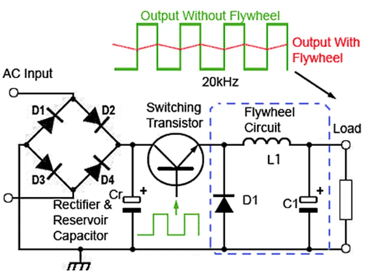
Fig.1.1 The Buck Converter
The Buck Converter
The Buck Converter is used in SMPS circuits where the DC output voltage needs to be lower than the DC input voltage. The DC input can be derived from rectified AC or from any DC supply. It is useful where electrical isolation is not needed between the switching circuit and the output, but where the input is from a rectified AC source, isolation between the AC source and the rectifier could be provided by the mains isolating transformer.
The switching transistor between the input and output of the Buck Converter continually switches on and off at high frequency. To maintain a continuous output, the circuit uses the energy stored in the inductor L, during the on periods of the switching transistor, to continue supplying the load during the off periods. The circuit operation depends on what is sometimes also called a Flywheel Circuit. This is because the circuit acts rather like a mechanical flywheel that, given regularly spaced pulses of energy keeps spinning smoothly (outputting energy) at a steady rate.
AC or DC Input
A buck converter is a form of DC to DC converter that can take input directly from a DC source, such as a battery. The input could also be DC derived from the AC mains (line) as shown in Fig. 3.1.1 via a rectifier/reservoir capacitor circuit. The AC input to the rectifier circuit could be AC at high voltage directly from the AC mains supply, or alternatively at a lower voltage via a step-down transformer. However the DC applied to the Buck Converter is obtained, it is then converted to a high-frequency AC, using a switching or ‘chopper’ transistor, driven by a (usually pulse width modulated) square wave. This results in a high-frequency AC wave, which can then be re-converted to DC in a much more efficient manner than would be possible in the circuits described in Power Supplies Module 1.
Buck Converter Operation
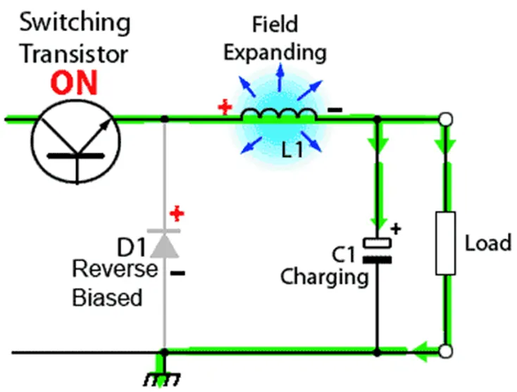
Fig.1.2 Switching Transistor ‘on’ Period
As shown in Fig. 3.1.1 the buck Converter circuit consists of the switching transistor, together with the flywheel circuit (Dl, L1 and C1). While the transistor is on, the current is flowing through the load via the inductor L1. The action of any inductor opposes changes in current flow and also acts as a store of energy. In this case, the switching transistor output is prevented from increasing immediately to its peak value as the inductor stores energy taken from the increasing output; this stored energy is later released back into the circuit as a back e.m.f. as current from the switching transistor is rapidly switched off.
Transistor Switch ‘on’ Period
In Fig. 3.1.2 therefore, when the switching transistor is switched on, it is supplying the load with the current. Initially, current flow to the load is restricted as energy is also being stored in L1, therefore the current in the load and the charge on C1 builds up gradually during the ‘on’ period. Notice that throughout the on period, there will be a large positive voltage on the D1 cathode and so the diode will be reverse biassed and therefore play no part in the action.
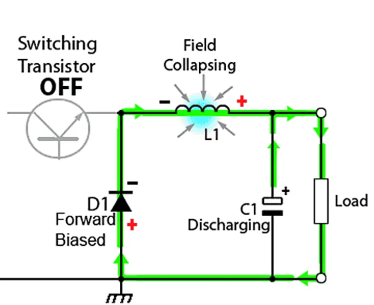
Fig. 1.3 Switching Transistor ‘off’ Period
2.Boost Converter
Switched-mode supplies can be used for many purposes including DC to DC converters. Often, although a DC supply, such as a battery may be available, its available voltage is not suitable for the system being supplied. For example, the motors used in driving electric automobiles require much higher voltages, in the region of 500V, than could be supplied by a battery alone. Even if banks of batteries were used, the extra weight and space taken up would be too great to be practical. The answer to this problem is to use fewer batteries and to boost the available DC voltage to the required level by using a boost converter. Another problem with batteries, large or small, is that their output voltage varies as the available charge is used up, and at some point, the battery voltage becomes too low to power the circuit is supplied. However, if this low output level can be boosted back up to a useful level again, by using a boost converter, the life of the battery can be extended.
The DC input to a boost converter can be from many sources as well as batteries, such as rectified AC from the mains supply, or DC from solar panels, fuel cells, dynamos and DC generators. The boost converter is different to the boost converter in that its output voltage is equal to, or greater than its input voltage. However, it is important to remember that, as power (P) = voltage (V) x current (I), if the output voltage is increased, the available output current must decrease.
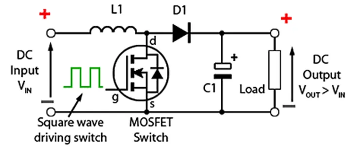
Fig.2.1 Basic Boost Converter Circuit
Fig. 3.2.1 illustrates the basic circuit of a Boost converter. However, in this example the switching transistor is a control MOSFET both bipolar power transistors and MOSFETs are used in power switching, the choice being determined by the current, voltage, switching speed and cost considerations. The rest of the components are the same as those used in the buck converter illustrated in Fig. 3.1.2, except that their positions have been rearranged.
Boost converter Operation
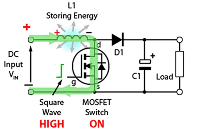
Fig. 3.2.2 Boost Converter Operation at Switch On
Fig 3.2.2 illustrates the circuit action during the initial high period of the high-frequency square wave applied to the MOSFET gate at startup. During this time MOSFET conducts, placing a short circuit from the right-hand side of L1 to the negative input supply terminal. Therefore a current flow between the positive and negative supply terminals through L1, which stores energy in its magnetic field. There is virtually no current flowing in the remainder of the circuit as the combination of D1, C1 and the load represent a much higher impedance than the path directly through the heavily conducting MOSFET.
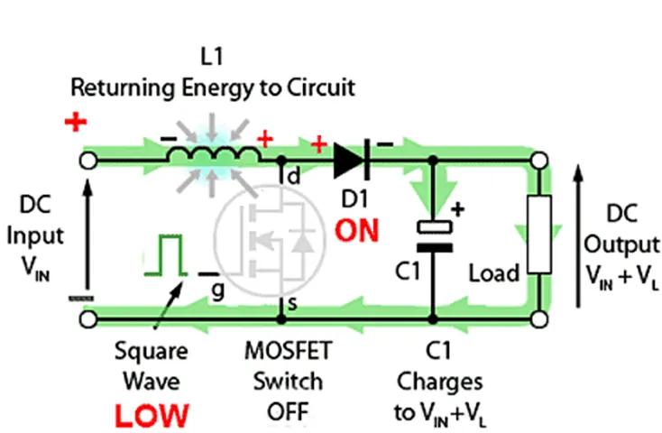
Fig. 3.2.3 Current Path with MOSFET Off
Fig. 3.2.3 shows the current path during the low period of the switching square wave cycle. As the MOSFET is rapidly turned off the sudden drop in current causes L1 to produce a back e.m.f in the opposite polarity to the voltage across L1 during the on period, to keep the current flowing. This results in two voltages, the supply voltage VIN and the back e.m.f.(VL) across L1 in series with each other.
This higher voltage (VIN +VL), now that there is no current path through the MOSFET, forward biases D1. The resulting current through D1 charges up C1 to VIN +VL minus the small forward voltage drop across D1, and also supplies the load.
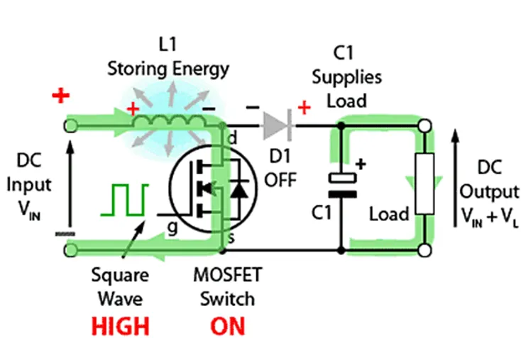
Fig. 2.4 Current Path with MOSFET On
Fig..2.4 shows the circuit action during MOSFET on periods after the initial start-up. Each time the MOSFET conducts, the cathode of D1 is more positive than its anode, due to the charge on C1. D1 is therefore turned off so the output of the circuit is isolated from the input, however, the load continues to be supplied with VIN +VL from the charge on C1. Although the charge C1 drains away through the load during this period, C1 is recharged each time the MOSFET switches off, so maintaining an almost steady output voltage across the load.
The theoretical DC output voltage is determined by the input voltage (VIN) divided by 1 minus the duty cycle (D) of the switching waveform, which will be some figure between 0 and 1 (corresponding to 0 to 100%) and therefore can be determined using the following formula:
3.Buck-Boost Converter
A Buck-Boost converter is a type of switched-mode power supply that combines the principles of the Buck Converter and the Boost converter in a single circuit. Like other SMPS designs, it provides a regulated DC output voltage from either an AC or a DC input.
The Buck converter described in Power Supplies Module 3.1 produces a DC output in a range from 0V to just less than the input voltage. The boost converter will produce an output voltage ranging from the same voltage as the input to a level much higher than the input.
There are many applications, however, such as battery-powered systems, where the input voltage can vary widely, starting at full charge and gradually decreasing as the battery charge is used up. At full charge, where the battery voltage may be higher than actually needed by the circuit being powered, a buck regulator would be ideal to keep the supply voltage steady. However, as the charge diminishes the input voltage falls below the level required by the circuit, and either the battery must be discarded or re-charged; at this point, the ideal alternative would be the boost regulator described in Power Supplies Module 3.2
By combining these two regulator designs it is possible to have a regulator circuit that can cope with a wide range of input voltages both higher or lower than that needed by the circuit. Fortunately, both buck and boost converters use very similar components; they just need to be re-arranged, depending on the level of the input voltage.
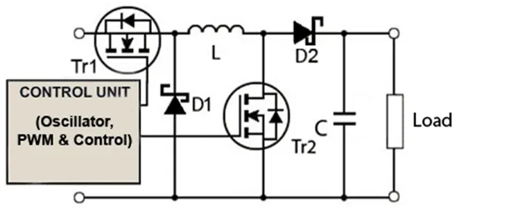
Fig. 3.1 Buck and Boost Converters Combined
In Fig. 3.3.1 the common components of the buck and boost circuits are combined. A control unit is added, which senses the level of input voltage, then selects the appropriate circuit action. (Note that in the examples in this section the transistors are shown as MOSFETs, commonly used in high-frequency power converters, and the diodes shown as Schottky types. These diodes have a low forward junction voltage when conducting, and are able to switch at high speeds).
Operation as a Buck Converter
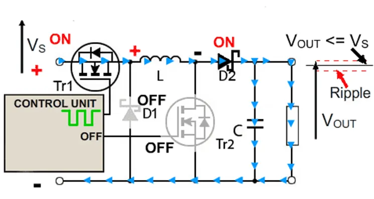
Fig. 3.2 Operation as a Buck Converter During Tr1 ‘on’ Period
The basic operation of the buck-boost converter is illustrated in Figs. 3.3.2 to 3.3.5
Fig. 3.3.2 shows the circuit operating as a Buck Converter. In this mode, Tr2 is turned off, and Tr1 is switched on and off by a high-frequency square wave from the control unit. When the gate of Tr1 is high, current flows through L, charging its magnetic field, charging C and supplying the load. The Schottky diode D1 is turned off due to the positive voltage on its cathode.
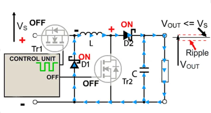
Fig. 3.3 Operation as a Buck Converter During Tr1 ‘off’ Period
Fig .3.3 shows the current flow during the buck operation of the circuit when the control unit switches Tr1 off. The initial source of current is now the inductor L. Its magnetic field is collapsing, the back e.m.f. generated by the collapsing field reverses the polarity of the voltage across L, which turns on D1 and current flows through D2 and the load.
As the current due to the discharge of L decreases, the charge accumulated in C during the period of Tr1 now also adds to the current flowing through the load, keeping VOUT reasonably constant during the off period. This helps keep the ripple amplitude to a minimum and VOUT close to the value of VS.
Operation as a Boost Converter
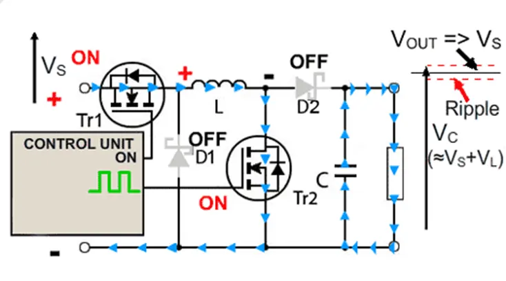
Fig. 3.4 Operation as a Boost Converter During Tr2 ‘on’ Period
In Boost Converter mode, Tr1 is turned on continually and the high-frequency square wave is applied to the Tr2 gate. During the on periods when Tr2 is conducting, the input current flows through the inductor L and via Tr2, directly back to the supply negative terminal charging up the magnetic field around L. Whilst this is happening D2 cannot conduct as its anode is being held at ground potential by the heavily conducting Tr2. For the duration of the on period, the load is being supplied entirely by the charge on the capacitor C, built upon previous oscillator cycles. The gradual discharge of C during the on a period (and its subsequent recharging) accounts for the amount of high-frequency ripple on the output voltage, which is at a potential of approximately VS + VL.
The Off Period
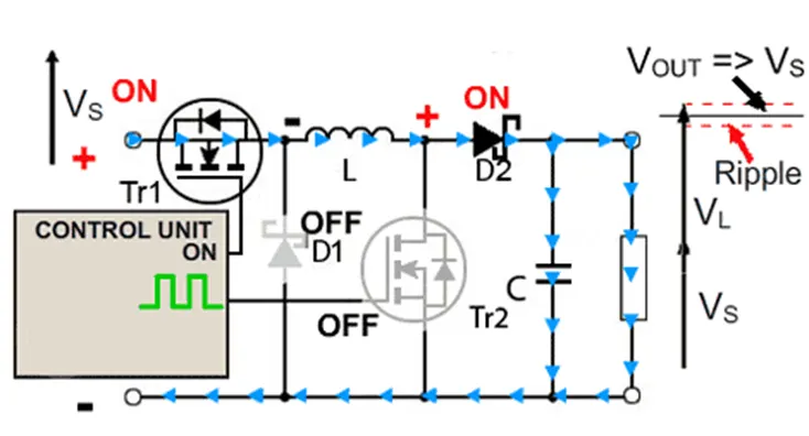
Fig. 3.5 Operation as a Boost Converter During Tr2 ‘off’ Period
At the start of the off period of Tr2, L is charged and C is partially discharged. The inductor L now generates a back e.m.f. and its value that depends on the rate of change of current as Tr2 switches of and on the amount of inductance the coil possesses; therefore the back e.m.f can be any voltage over a wide range, depending on the design of the circuit. Notice particularly that the polarity of the voltage across L has now reversed, and so adds to the input voltage VS giving an output voltage that is at least equal to or greater than the input voltage. D2 is now forward biased and so the circuit current supplies the load current, and at the same time re-charges the capacitor to VS + VL ready for the next on-period of Tr2.
3)DC TO AC CONVERTER
An inverter is a device that converts DC power from the battery to AC power used in an electric vehicle motor. The inverter can change the speed at which the motor rotates by adjusting the frequency of the alternating current.
The use of Inverters can increase or decrease the power or torque of the Engine the motor by adjusting the amplitude of the signal. It plays a significant role in capturing energy from regenerative braking and feeding it back to the battery. The output voltage waveform of ideal inverters should be sinusoidal, However, the waveform of practical inverters are non-sinusoidal and contain certain harmonics
1) AC T0 DC CONVERTER RECTIFIER-USED IN EV CHARGER
2) DC TO DE CONVERTER (CHOPPER-ED TO SUPPLY DC POMEN 10 AUSARY LEAD AND CAR HEADLIGHTS
3) DC T0 AC CONVERTER INVERTERS-SED TO SUPPLY POWER TO MASTER
Question 2
An Electric Vehicle's powertrain with a 72V battery pack is shown in the diagram below. The duty ratio for acceleration operation is 'd1' and for the braking operation the duty ratio is 'd2'.
The other parameters of the electric vehicle are given below,
Motor and Controller Parameters:
Rated Armature voltage= 72 V
Rated armature current= 400 A
Ra= 0.5Ω,
KΦ= 0.7 Volt second
Chopper Switching frequency= 400 Hz
The vehicle speed-torque characteristics are given by the below equation
What is EV steady-state speed if the duty cycle is 70%?
Solution:-
vehicle output voltage (Vv) is given by:_
Vv=Battery voltage (V)*Duty cycle
Vv=72*0.70
Thus vehicle voltage =50.04
Now Equation for vehicle torque is given by

T= Vehicle Torque (N-m)
V= Vehicle voltage (Volts)
ω =steady-state speed of the vehicle (rps)
K=Motor constant
Ra=Armature Resistance
Substituting all these values in the equation, we get:
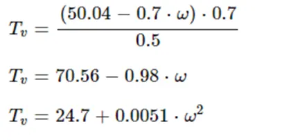
Solving these two equations.
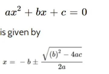
We get a quadratic equation

since the quadratic equation, we get two values

we have taken positive value
steady-state speed of the vehicle (rps)=38.85 rps
Question 3
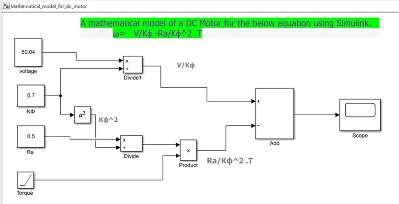
ω= V/Kϕ -Ra/Kϕ^2.T
let us draw a model for the above equation as shown below.
let
V=50.4 volts
Kϕ=0.7
Ra=0.5 ohms
let us consider torque as a linearly increasing signalled that is equal to the ram block of the following Simulink model
thus we find that, for the fixed voltage,
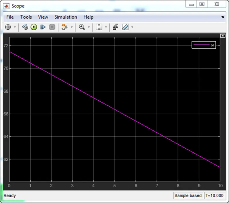
the speed of the motor is inversely proportional to load this means that increase in load torque will result in a decrease in speed.
Question 4
- Refer to the blog on the below topic Induction Versus DC brushless motors by Wally Rippel, Tesla Explain in brief about author's perspective. The following points can be concluded from the above topic:
- In the first place, the creator portrays the predominance of Internal Combustion Engines (ICE) in the realm of the auto business and furthermore examine various sorts of motors. He clarifies that all motors were comparative and it was dependent upon the client to choose as indicated by their necessity. He additionally talks about enlistment engines and brushless DC engines and presents his view that these two innovations will be broadly utilized in the coming years.
- Then he clarifies the working of both a 3-stage enlistment engine and a brushless DC engine. . Presently the creator has done a correlation between these two innovations and expressed a few benefits and burdens of each.
- Induction engine enjoys a few benefits like it has no magnets The engine can turn over under load. No inverter is required. A few disservices of Induction engines are: They can't work from DC: AC is an absolute necessity. Shaft speed is proportionate to line recurrence. Consequently, when utilized with utility force, they are steady speed machines. When worked from utility force, they have restricted beginning force and fairly restricted running pinnacle force abilities, when contrasted with DC type machines
- Brushless DC engine enjoys a few benefits like considerably less rotor heat is produced with the DC brushless drive. The pinnacle point energy productivity for a DC brushless drive will normally be a couple of rate focuses higher than for an acceptance drive. A few drawbacks of a Brushless DC engine are: as machine size develops. the attractive misfortunes increment proportionately and part load proficiency drops. Perpetual magnets are costly and hard to deal with because of extremely enormous powers that become an integral factor when anything ferromagnetic draws near to them.
- Finally, the creator couldn't pick which drive is superior to the next however clarifies that DC brushless drives will probably keep on overwhelming in the crossbreed and coming module half breed markets, and that enlistment drives will probably keep up with strength for the elite unadulterated electrics