Project 2 - SiC/IGBT isolated gate driver reference design with thermal diode and sensing FET
1) This is the schematic diagram for the given question :
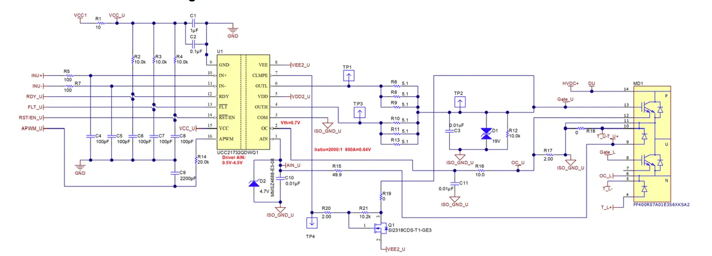
Based on the schematic ,we should go with multilayers.
Multilayer PCB : Modern electronics cannot work without multilayer PCBs, which allow designers to pack more complexity and functionality into smaller form factors. Several layers of conducting traces and insulating material are laminated to form a single integrated circuit board on a multilayer PCB.
The design of a multilayer PCB is a complex and iterative process that includes defining the dimensions, layers, and materials, deciding on the signal and power layers, establishing PCB layers and assigning regions, figuring out the PCB stack-up order, drawing the PCB layout and routing, verifying the design through circuit simulation, electrical checks, and prototyping, selecting the best PCB manufacturer, and taking EMC and safety into account.
Signal integrity, power supply, and EMI are all impacted by the stack-up order, which is essential for the PCB's performance. Crosstalk and signal degradation are minimized, EMI is decreased, and power delivery is optimized with a well-designed stack-up sequence. Meeting the functional, performance, and cost requirements of modern electronics also depends on choosing the proper stack-up sequence.
Criteria for selecting the right stack-up order :
The proper stack-up sequence must be chosen based on the PCB design's specific demands, including the number of layers, signal speeds, power needs, and thermal management. The following are some factors for choosing the appropriate stack-up order:
Signal integrity: Signal loss, crosstalk, and degradation should be minimized by the stack-up sequence. To reduce EMI and provide shielding, the signal layers should be positioned in between the ground and power planes.
Power delivery: To provide proper power supply to all components, eliminate voltage dips, and lower power plane noise, the stack-up sequence should be followed. The power planes should be distributed as needed and positioned next to the ground planes.
Thermal management: The PCB's thermal characteristics, such as heat dissipation, thermal conductivity, and thermal expansion, should be taken into account while determining the stack-up sequence. The PCB should be built to effectively disperse heat, prevent hotspots, and lessen the possibility of delamination.
If you are going with the multilayer configurations. Need to consider few things
Negative plane layers: Ground and power planes on multilayer PCB layouts are frequently created using negative image plane layers. For drilled holes on a negative plane layer, several CAD programs require clearances to be included into the pad and footprint forms. Make sure your pad and footprint shapes are configured with the proper negative plane clearances if you're using one of these pcb design software packages. You will end up with a short if your shapes are not configured for these clearances.
Inner signal layer pad shapes: Some designs employ different inner layer pad shapes than they use outer layer pad shapes. For visual identification purposes, pin 1 pads, for example, frequently have a square form rather than the round shape that it typically has on inner layers. Your libraries might not produce the correct pad shapes on inner signal layers if they are not configured for multi-layer pcb setups.
2) a) PCB Trace : The role of a PCB is to conduct signals and data from one point to another. To achieve this, the signals must travel on a path. PCB traces act as the transmission paths for these signals and data. They link various PCB components, such as the IC, capacitors, and resistors. Therefore, without traces, a PCB cannot function properly.
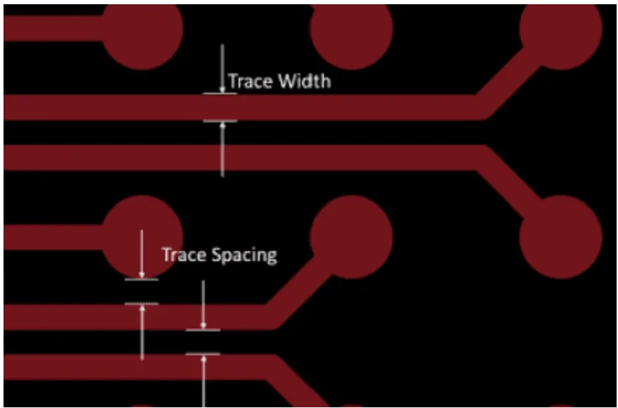
Since the transmitted signals are made up of electric current, the materials used to create the traces must be both good electrical conductors and sufficiently stable. Copper foil is a typical material used to create PCB traces.
Trace Width : The trace width is basically the width of the copper foil, measured in mils – 0.0254 mm. Miscalculating the width might burn the trace.
We can solve trace width using formaula or pcb trace width calculator.
First method :
PCB Trace Width using formula :
Applying the trace width equation is the most effective technique to determine the PCB trace width. You may use the formula to get the proper current that can flow through a particular trace. The IPC 2221 trace width formula is given below:
I=k*ΔT^0.44*A^0.725
I is the current, and it is always constant. ΔT is the temperature change, and A is the cross-sectional area.
You can restructure the above equation to have the trace width on the left-hand side as shown below:
Area [mils^2] = (Current [Amps]/ (k*(Temp_Rise [deg. C]) ^ 0.44)) ^ (1/0.725)
However, to create the right width, you must consider your trace thickness.
Width [mils] = Area [mils^2]/ (Thickness [oz]*1.378[mils/oz])
Second Method :
In saturn PCB software we can calculate trace width. First step is go to Conductor properties. After opening conductor properties these dialog box will appear:
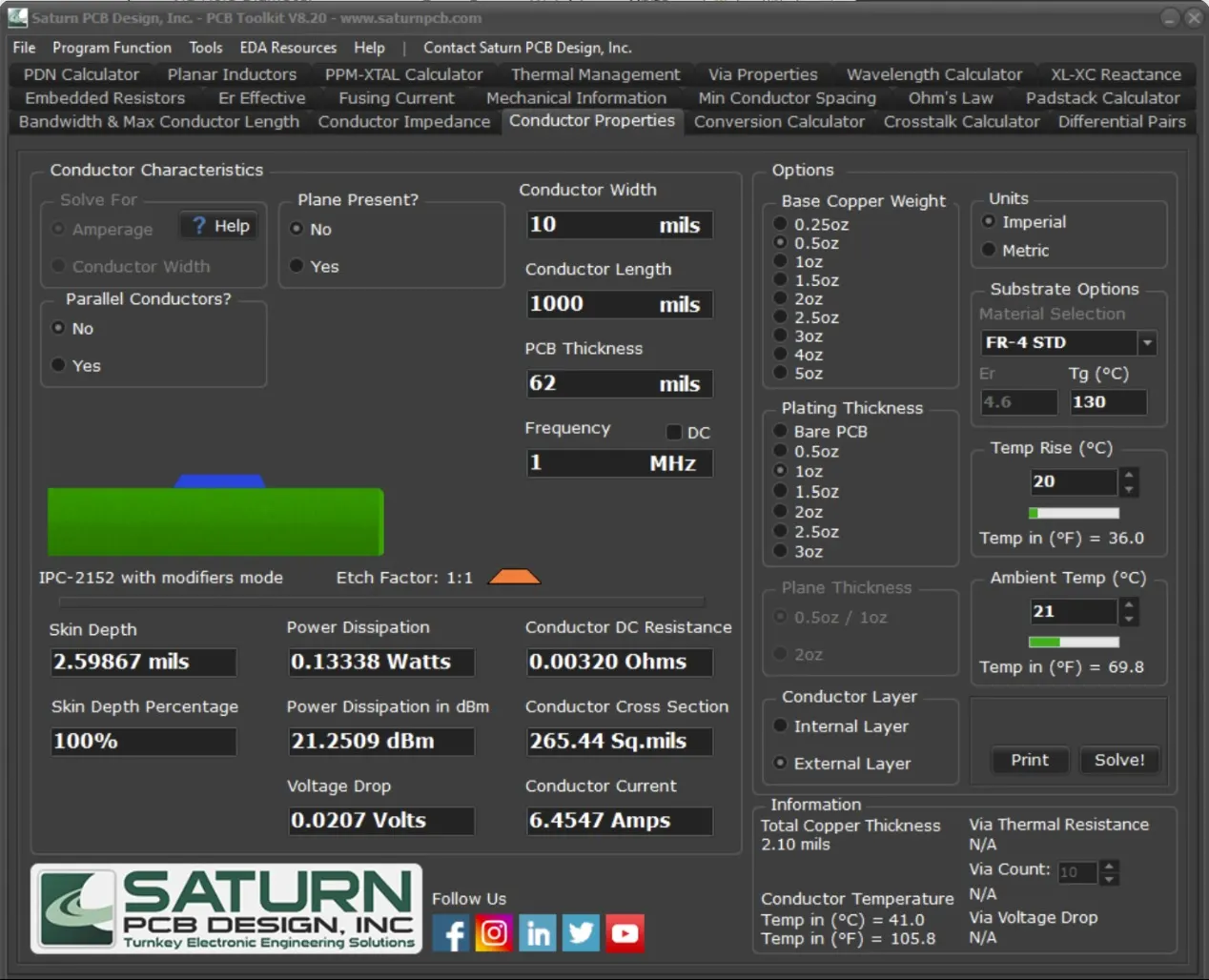
Amperage: Sets solving for amperage as the priority where conductor width is the input.
Conductor Width: Sets solving for conductor width as the priority where amperage is the input.
This selection is only enabled for the IPC-2152 Without Modifiers and the IPC-2221 options.
Conductor Layer: Select between an internal or external conductor.
Plane Present: Select if a plane is present in your design. A copper plane will help dissipate heat away from the conductor.
Plane Thickness: Select between one of the two preset thicknesses for the plane. This tool cannot determine with accuracy a plane greater than 2oz. thick.
Distance to Plane: If Plane Present is set to “Yes”, this option becomes available. Enter the distance between the conductor and plane.
Parallel Conductors: Select when trying to determine the effect of parallel conductors on current vs temperature rise.
Parallel Conductor Count: If Parallel Conductors is set to “Yes”, this option becomes available. Enter the number of parallel conductors to be factored in.
Conductor Width: Enter the width of the conductor.
Conductor Length: Enter the length of the conductor.
PCB Thickness: Enter the overall thickness of the PCB. The thickness of the PCB plays a role in current vs temperature rise as the substrate acts as a heat sink.
Frequency: Enter the frequency, if any, of a signal through the conductor. The field is only necessary for skin depth and has no influence on current vs temperature rise.
Load Current: Enter the load current flowing through the conductor. NOTE: This is separate from “Conductor Current” which is a calculated value based on temperature rise. Entering a load current allows the tool to find the voltage drop and temperature of a conductor based on the entered value.
Conductor DC Resistance: This is the DC resistance of the conductor based on its width and length.
Total Cross Section: This is the area of a cross section of the conductor. This can change with etch factor as is used to determine conductor current.
Temp Rise: Set the maximum temperature rise allowed in the conductor by way of current flowing through it.
Ambient Temp: Set the ambient temperature of the PCB, this will be added to temp rise to determine the total temperature of the conductor once current flows through it.
Conductor Current: This is the calculated amount of current that will cause the temperature of the conductor to rise, above ambient, to the set temperature. This IS NOT the maximum current the conductor can handle before burning up. In the above example, 4.381A will cause a 50mil wide conductor to rise 20C above ambient.
If the ambient temperature + temp rise selected is greater than the selected material’s Tg value, a warning will appear stating that the maximum material temperature has been exceeded.
Distance to Plane: If Plane Present is set to “Yes”, this option becomes available. Enter the distance between the conductor and plane.
Power Dissipation: This is the power dissipated by the conductor based on DC resistance and voltage drop.
Power Dissipation in dBm: This is the power dissipated by the conductor based on DC resistance and voltage drop expressed in decibels.
Voltage Drop:This is the voltage drop across the conductor based on the derived values of current and DC resistance.
Loaded Voltage Drop: This is the loaded voltage drop across the conductor based on the entered values of load current and the derived value of DC resistance
b) Via Size : We can calculate using Saturn PCB
These is the dialog box appears when you go for Via properties
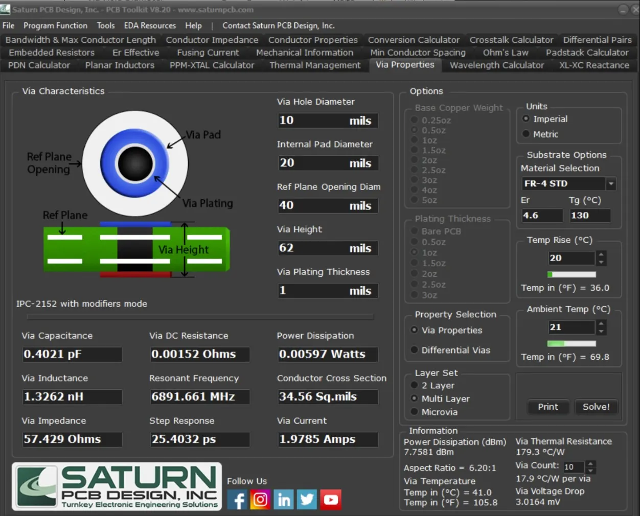
Layer Set: Choose between a 2 layer via, a multi-layer via and a microvia.
Via Hole Diameter: This is the finished diameter the via hole.
Internal Pad Diameter: This is the diameter of the inner layer pad for the via and is used for multi-layer impedance calculations.
Reference Plane Opening Diameter: This is the diameter of the opening surrounding the internal pad. This value can’t be less than internal pad diameter.
Via Height: This is the length of the via from its starting layer to its ending layer. The thinner a PCB is, the less heat it can dissipate thereby lowering the current needed in a via to raise its temperature.
Via Plating Thickness: This is the thickness of copper plated into the via hole after drilling. Ask your vendor for the exact value to get a more accurate result as this value can vary.
Via Capacitance: This is the approximated capacitance of the via with the given inputs. This value is only available for multi-layer vias as it uses the internal pad and reference plane opening for the calculation.
Via Inductance: This is the approximated inductance of the via with the given inputs.
Via Impedance:This is the approximated AC impedance of the via with the given inputs. This value is only available for multi-layer vias as it uses via capacitance for the calculation. via_zo = sqrt(via_l/ (via_c * 0.001))
Via DC Resistance:This is the approximated DC resistance of the via with the given inputs.
Resonant Frequency:This is the approximated resonant frequency of the via with the given inputs. This value is only available for multi-layer vias as it uses the via capacitance for the calculation.
Power Dissipation: This is the approximated power dissipation of the via with the given inputs. It is found by the I2R method using the calculated values of via current and DC resistance.
c) Trace length : longer traces create a high resistance, implying that length is also an important PCB trace resistance consideration. You should aim to design a small board by minimizing the length of the traces. Though you will end up with short and wide traces, your PCB will have the quickest signal transmission time.
In reality, there is no single formula for calculating the exact trace length you need in your printed circuit board. When your PCB design software includes an automated trace length calculator, you can immediately view lengths for individual traces or for all traces in a net. You’ll be able to check your trace lengths against the propagation delay tolerances in your traces.
In Altium design , we can see the trace length on left side of the screen .If you want to see for the trace length for any particular net. Select the net , left side of the screen go for Routed length option .
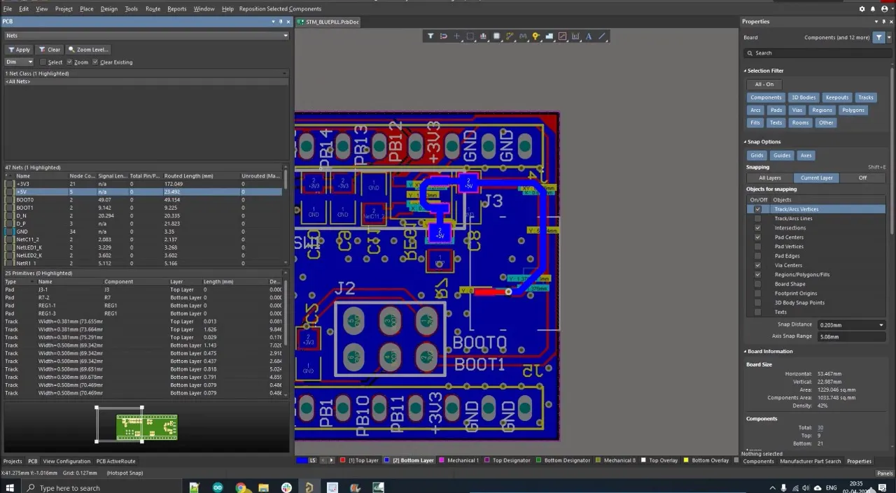
3)
The majority of electronic components release heat whenever a current passes through them. The power, device characteristics, and circuit design all affect how much heat is produced. In addition to the components, some heat and power losses are caused by the resistance of the electrical connections, copper traces, and vias.
The goal for designers should be to create PCBs that run and maintain acceptable temperature ranges in order to prevent failures or circuit malfunctions. There are circumstances where adding heat sinks, cooling fans, or a combination of various techniques is unavoidable, even if certain circuits can function without extra cooling.
Major issues to consider during design are:
- Performance data and dimensions of the components
- Major heat-dissipating components
- Size of the PCB
- PCB material, layout, and component placement
- Mounting peripherals
- Temperature of the application environment
- Amount of heat dissipated
- Appropriate cooling methods, i.e., cooling fans, heat sink, etc.
Several methods of PCB heat dissipation are available to designers:
1) Heat Sinks
Due to the numerous heat-producing components it includes, a PCB is essentially a factory that produces heat. There must be a mechanism for the PCB to release all of that thermal energy. Typically, heat sinks are the solution. Heat sinks securely move the heat to prevent it from building up and harming the board.
2) Fans
The majority of electronic equipment include fans for cooling, and one of those fans' functions is to assist in cooling PCBs. Cooling fans circulate cold air into electrical equipment while removing heat from them, preventing overheating and enhancing PCB performance and durability.
3) Considering Materials and Components
One of the best methods for lowering heat in a PCB is to use materials that are heat resistant. For instance, heavy copper PCBs made from thick copper plates are a great option due to their robustness and capacity to resist high temperatures. Compared to normal PCBs, they can manage larger currents, tolerate higher temperatures for longer periods of time, and offer stronger connecting points. They are especially helpful in heavy-duty situations such as those found in the automotive, aircraft, heavy machinery, power converter, and other industries.
4) Increasing Plate Width and Thickness
Thicker plates in PCBs often transfer heat less efficiently than thinner ones. With the proper engineering, they can help lower the possibility of overheating, wraping, and disruption since they need more power to attain high temperatures.
5) Applying Laminates
Another strategy for avoiding damage from high temperatures is to apply laminates. The components of the PCB can be provided with heat protection via high-temperature PCB laminates, which can stop overheating.
The following precautions should be present in high-temperature laminates:
- Glass transition temperature (TG)
- Time to delamination
- Moisture absorption
- Decomposition temperature (TD)
- Z-axis expansion
6) Aligning CTEs
When a material is subjected to high temperatures, its coefficient of thermal expansion (CTE) calculates how much it expands. It's preferable in PCB design for the dielectric layers to have a CTE that is comparable to the copper layers'. If the layers do expand, they will do so uniformly, causing the least amount of harm possible.
7) Maintaining Adequate Spacing
It might be difficult to determine the distance between components on a PCB. When board components are too close together, crosstalk may result — that is, different components may begin interacting with each other in undesirable ways. The skin impact is a result of these undesirable interactions. The skin effect causes trace resistances to rise, which causes resistive losses and heat buildup in the circuit. Engineers must be very careful with component spacing on high-frequency PCBs since the skin effect is particularly frequent with these boards.
8) Integrating Heat Pipes Correctly
A PCB may have heat pipes that could help in heat distribution. Heat can be absorbed by the liquid in the pipes, protecting the board's components from damage.
9) Maximizing RTI and MOT
Maximum operating temperature (MOT) and Relative thermal index (RTI) are two important parameters that engineers should carefully consider while designing PCBs. RTI indicates the highest temperature that a material can handle without undergoing changes to its properties or a reduction in its performance.
4) Advantage of Multilayer PCB :
Size : A multi-layer PCB is thicker, but one board may frequently replace several other boards, thus there is no need for a space that can accommodate several boards. One of the most crucial advantages of the multi-layer PCB is its ability to accommodate more connections into a smaller area. The smaller a device may be in today's electronics industry, the better, and multi-layer printed circuit boards significantly contribute to satisfying this need.
Weight : Related closely to a smaller size, a lighter weight product is also in high demand in today’s electronics marketplaces. In the multi-layer design, the need to connect multiple single PCBs is eliminated for the lighter option of a single multi-layer PCB.
Cost : When multiple PCBs can be condensed into 1 circuit board it can save money in the long run. Set up and processing time for multiple boards is lessened, parts for connections from circuit board to circuit board are taken out of the equation and generally overall component pricing will can be reduced by moving from more than 1 single layer PCBs to 1 multi-layer PCB. Switching to a multi-layer design can be extremely cost saving on long term large run designs.
The nature and benefits of multi-layer PCBs have made them desirable in such products as cell phones, heart monitors, x-ray machines, GPS technology, and computers. Mobile devices, in particular, prefer multi-layer PCBs, as do a number of industry-specific applications.