Project 1 - 40-V to 80-V adjustable output voltage boost reference design for LIDAR applications
1) This is the schematic diagram for the given question :
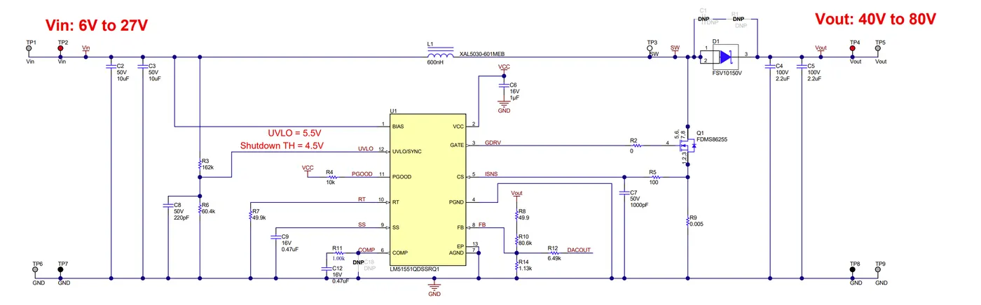
Based on the schematic , we can decide the layers.
According to the schematic , double layers PCB suits correctly.
Reasons for not choosing single layer PCB :
- Circuits that need high speed or high density cannot be built on a single-layer PCB.
- It does not provide sufficient space for complex systems or multiple components.
- It uses much less room than a double-sided PCB.
- Compared to multi-layer PCBs, it is bigger and heavier.
- Electromagnetic interference is more likely to affect a single-sided PCB.
- Signal routing is more challenging on a single-sided PCB.
Double Layer PCB :
Electrical connections and mechanical support are both possible for components on the two sides of double-sided printed circuit boards. Holes, referred to as vias, are drilled through the board and are lined with copper. These enable connections between circuits on both sides of the board.
The space on 2-layer PCBs is more than enough for a ground grid, which significantly lowers electrical noise. They are more widely used than single layer printed circuit boards because they are less expensive, offer more area for components, and make routing considerably simpler.
Advantages of double layer PCB :
Compact Density:
Due to the high compact density of double-layered PCBs, more components may be conveniently packed into a small area. We may insert the components on both the upper and bottom sides as both PCBs are in use.
In order to increase the board's compactness and improve its functionality, we use both sides of the board. In contrast, a single-sided board just has one side used, hence it cannot be used for complex uses.
Occupies Less Space:
Even though it has two layers, it takes up less space than a PCB with just one layer. Each component is properly utilized becaue of its great density and compactness.
Fabrication:
The circuit board of a double-layer PCB is excellent for difficult design applications because it contains metal on both sides, a high transition temperature Cu board, flexibility, and high frequency. For the purpose of creating double-layer PCB board models, several surface treatments are carried out. These methods involve spraying Pb-free sn and immersion gold.
2)
a) PCB Trace : The role of a PCB is to conduct signals and data from one point to another. To achieve this, the signals must travel on a path. PCB traces act as the transmission paths for these signals and data. They link various PCB components, such as the IC, capacitors, and resistors. Therefore, without traces, a PCB cannot function properly.
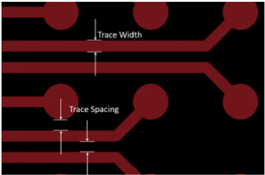
Since the transmitted signals are made up of electric current, the materials used to create the traces must be both good electrical conductors and sufficiently stable. Copper foil is a typical material used to create PCB traces.
Trace Width : The trace width is basically the width of the copper foil, measured in mils – 0.0254 mm. Miscalculating the width might burn the trace.
We can solve trace width using formaula or pcb trace width calculator.
First method :
PCB Trace Width using formula :
Applying the trace width equation is the most effective technique to determine the PCB trace width. You may use the formula to get the proper current that can flow through a particular trace. The IPC 2221 trace width formula is given below:
I=k*ΔT^0.44*A^0.725
I is the current, and it is always constant. ΔT is the temperature change, and A is the cross-sectional area.
You can restructure the above equation to have the trace width on the left-hand side as shown below:
Area [mils^2] = (Current [Amps]/ (k*(Temp_Rise [deg. C]) ^ 0.44)) ^ (1/0.725)
However, to create the right width, you must consider your trace thickness.
Width [mils] = Area [mils^2]/ (Thickness [oz]*1.378[mils/oz])
Second Method :
In saturn PCB software we can calculate trace width. First step is go to Conductor properties. After opening conductor properties these dialog box will appear:
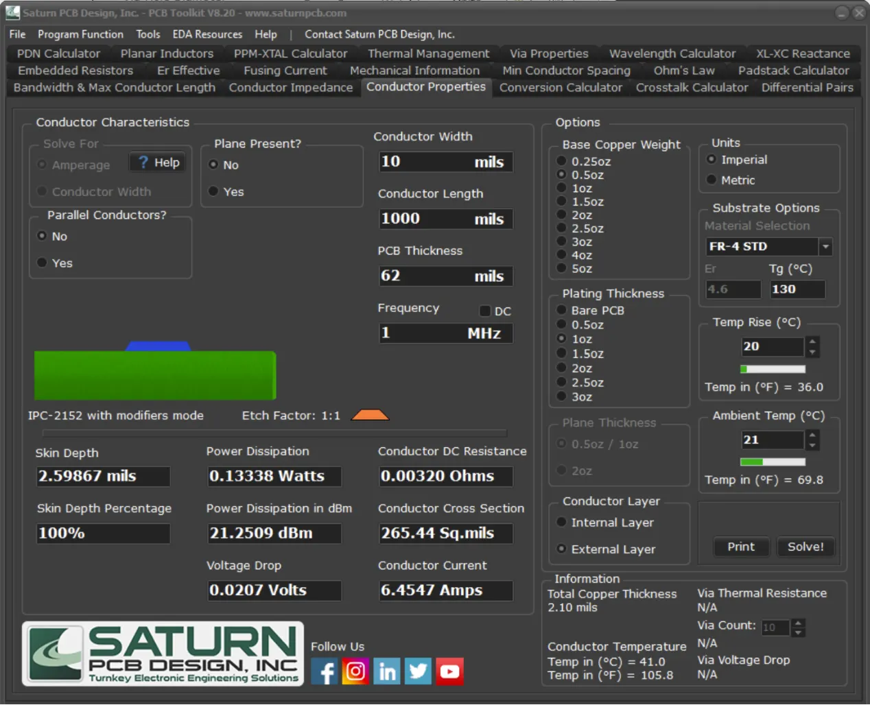
Amperage: Sets solving for amperage as the priority where conductor width is the input.
Conductor Width: Sets solving for conductor width as the priority where amperage is the input.
This selection is only enabled for the IPC-2152 Without Modifiers and the IPC-2221 options.
Conductor Layer: Select between an internal or external conductor.
Plane Present: Select if a plane is present in your design. A copper plane will help dissipate heat away from the conductor.
Plane Thickness: Select between one of the two preset thicknesses for the plane. This tool cannot determine with accuracy a plane greater than 2oz. thick.
Distance to Plane: If Plane Present is set to “Yes”, this option becomes available. Enter the distance between the conductor and plane.
Parallel Conductors: Select when trying to determine the effect of parallel conductors on current vs temperature rise.
Parallel Conductor Count: If Parallel Conductors is set to “Yes”, this option becomes available. Enter the number of parallel conductors to be factored in.
Conductor Width: Enter the width of the conductor.
Conductor Length: Enter the length of the conductor.
PCB Thickness: Enter the overall thickness of the PCB. The thickness of the PCB plays a role in current vs temperature rise as the substrate acts as a heat sink.
Frequency: Enter the frequency, if any, of a signal through the conductor. The field is only necessary for skin depth and has no influence on current vs temperature rise.
Load Current: Enter the load current flowing through the conductor. NOTE: This is separate from “Conductor Current” which is a calculated value based on temperature rise. Entering a load current allows the tool to find the voltage drop and temperature of a conductor based on the entered value.
Conductor DC Resistance: This is the DC resistance of the conductor based on its width and length.
Total Cross Section: This is the area of a cross section of the conductor. This can change with etch factor as is used to determine conductor current.
Temp Rise: Set the maximum temperature rise allowed in the conductor by way of current flowing through it.
Ambient Temp: Set the ambient temperature of the PCB, this will be added to temp rise to determine the total temperature of the conductor once current flows through it.
Conductor Current: This is the calculated amount of current that will cause the temperature of the conductor to rise, above ambient, to the set temperature. This IS NOT the maximum current the conductor can handle before burning up. In the above example, 4.381A will cause a 50mil wide conductor to rise 20C above ambient.
If the ambient temperature + temp rise selected is greater than the selected material’s Tg value, a warning will appear stating that the maximum material temperature has been exceeded.
Distance to Plane: If Plane Present is set to “Yes”, this option becomes available. Enter the distance between the conductor and plane.
Power Dissipation: This is the power dissipated by the conductor based on DC resistance and voltage drop.
Power Dissipation in dBm: This is the power dissipated by the conductor based on DC resistance and voltage drop expressed in decibels.
Voltage Drop:This is the voltage drop across the conductor based on the derived values of current and DC resistance.
Loaded Voltage Drop: This is the loaded voltage drop across the conductor based on the entered values of load current and the derived value of DC resistance
b) Via Size : We can calculate using Saturn PCB
These is the dialog box appears when you go for Via properties
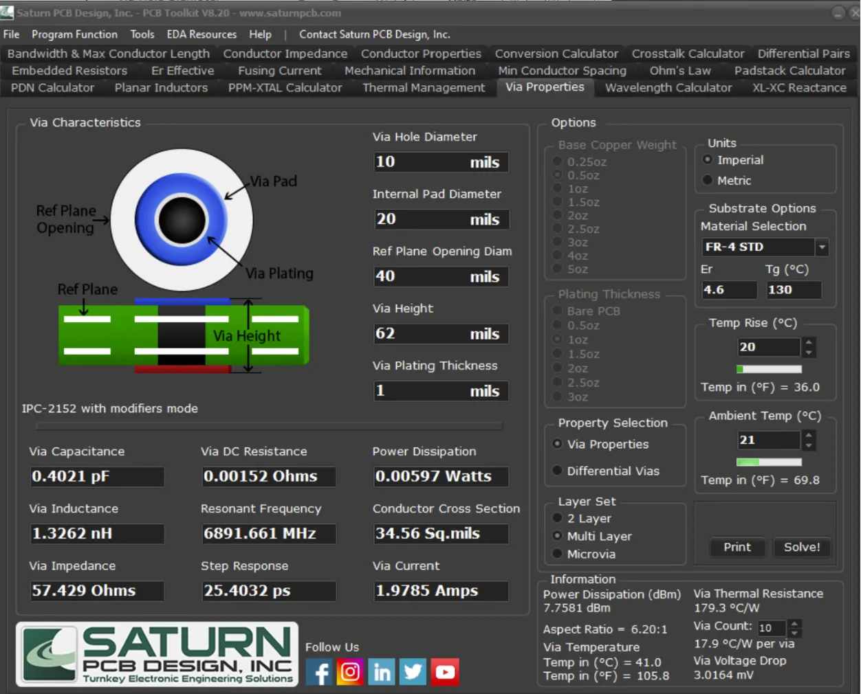
Layer Set: Choose between a 2 layer via, a multi-layer via and a microvia.
Via Hole Diameter: This is the finished diameter the via hole.
Internal Pad Diameter: This is the diameter of the inner layer pad for the via and is used for multi-layer impedance calculations.
Reference Plane Opening Diameter: This is the diameter of the opening surrounding the internal pad. This value can’t be less than internal pad diameter.
Via Height: This is the length of the via from its starting layer to its ending layer. The thinner a PCB is, the less heat it can dissipate thereby lowering the current needed in a via to raise its temperature.
Via Plating Thickness: This is the thickness of copper plated into the via hole after drilling. Ask your vendor for the exact value to get a more accurate result as this value can vary.
Via Capacitance: This is the approximated capacitance of the via with the given inputs. This value is only available for multi-layer vias as it uses the internal pad and reference plane opening for the calculation.
Via Inductance: This is the approximated inductance of the via with the given inputs.
Via Impedance:This is the approximated AC impedance of the via with the given inputs. This value is only available for multi-layer vias as it uses via capacitance for the calculation. via_zo = sqrt(via_l/ (via_c * 0.001))
Via DC Resistance:This is the approximated DC resistance of the via with the given inputs.
Resonant Frequency:This is the approximated resonant frequency of the via with the given inputs. This value is only available for multi-layer vias as it uses the via capacitance for the calculation.
Power Dissipation: This is the approximated power dissipation of the via with the given inputs. It is found by the I2R method using the calculated values of via current and DC resistance.
c) Trace length : longer traces create a high resistance, implying that length is also an important PCB trace resistance consideration. You should aim to design a small board by minimizing the length of the traces. Though you will end up with short and wide traces, your PCB will have the quickest signal transmission time.
In reality, there is no single formula for calculating the exact trace length you need in your printed circuit board. When your PCB design software includes an automated trace length calculator, you can immediately view lengths for individual traces or for all traces in a net. You’ll be able to check your trace lengths against the propagation delay tolerances in your traces.
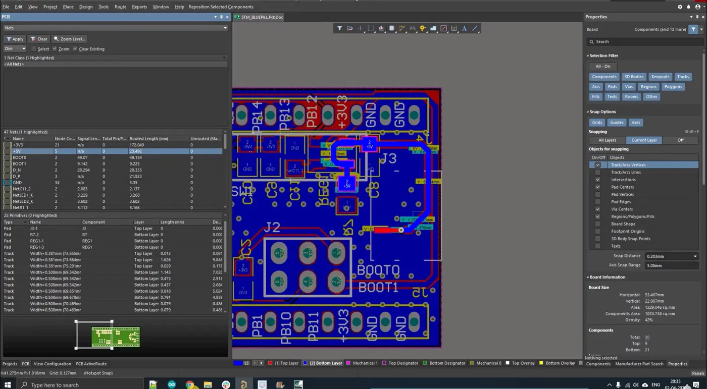
In Altium design , we can see the trace length on left side of the screen .If you want to see for the trace length for any particular net. Select the net , left side of the screen go for Routed length option .
3) Disadvantages of 2 layer pcb :
Compared to other PCB types, 2 Layer PCBs are also susceptible to crosstalk and noise.
- They cost more to produce than single-sided boards.
- Additionally, they have a lengthier manufacturing production process since they need additional solder mask layers.
- Also, soldering through-hole vias might be challenging.
- Furthermore, it is more difficult to manufacture double-sided PCBs than single-sided PCBs.
- Last but not least, double-sided PCB has a lower yield rate than single-sided PCB.
In short, double-sided PCB drawbacks include greater cost, lengthier manufacturing process, more challenging soldering, and lower yield rate.