Project 2
Problem statements:
Part A:
- Design a DC power supply using PFC circuit for general purpose applications with 350V dc output and load in the range of 0-7A. The supply should meet the harmonic standard limits for input power quality such that current THD limits are satisfied with input power factor >0.97 value. The input side is connected to single phase grid with parameters as 230V, 50Hz.
Design the supply to give following specifications:
The Boost Power Factor Correction Converter
One of the most common active PFC circuits is called the boost PFC converter, which is a relatively simple and low-cost circuit. The only extra components that are required beyond the ones used in a linear AC-DC converter are a switch (usually a FET), a diode, and an inductor.
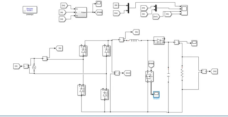
Figure 1 below shows a boost PFC converter. You can see that it is essentially a linear power supply with a boost converter inserted between the rectifier and the filter capacitor.
Figure 1. Boost PFC converter circuit
The general goal of the boost PFC converter is to turn the switch (S1) off and on rapidly and with a varying duty cycle in order to make the input current (iac) sinusoidal and in phase with the input voltage (vac).
Boost PFC Converter Operation
The boost PFC circuit cycles rapidly between two states. The first state occurs when S1 is closed, as shown in Figure 2. When in this state, the inductor is being energized by the AC side of the circuit via the rectifier, and thus the inductor current will be increasing. At the same time, diode Dpfc becomes reverse biased (because its anode is connected to ground through S1), and energy is provided to the load by the capacitor.
Figure 2. Boost PFC converter with the switch (S1) closed
Figure 3 shows the second state, which occurs when S1 is open. In this state, the inductor de-energizes (the current decreases) as it supplies energy to the load and for recharging the capacitor.
Figure 3. Boost PFC converter with the switch (S1) open
(Note that both Figure 2 and Figure 3 show only the positive half of the input voltage cycle. The negative half would be identical except that current would be flowing through the other two diodes of the rectifier.)
The cycling between the two states is done at a high frequency that is at least in the tens of kHz, but is often an order of magnitude (or even more) higher than that. The cycling back and forth between states is done rapidly and in a manner that both maintains a constant output voltage and controls the average inductor current (and subsequently the average AC current).
Since the inductor current is increasing in state 1 and decreasing in state 2, the duty cycle determines the amount of time the inductor current increases versus the amount of time the inductor current decreases. Thus, by varying the duty cycle, the average inductor current can be adjusted. By making this average current track the expected current, you can get a significant improvement in power factor and total harmonic distortion (THD).
For an ideal system, the expected inductor current would be a rectified sine wave and the expected AC input current would be a sine wave. Because of the switching nature of the system and the difficulty in obtaining perfect tracking of the expected current, the AC input current (Iac) will not be an ideal sine wave and the inductor current (I(L)) will not be an ideal rectified sine wave, but will instead look something like this:
- Component selection and justification
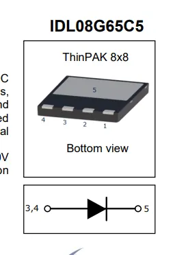
for rectifire and boost diode here we have select silicon carbide diode of IDL08G65C5 of INFINEON TECHNOLOGY

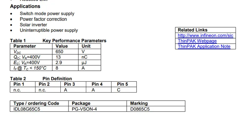
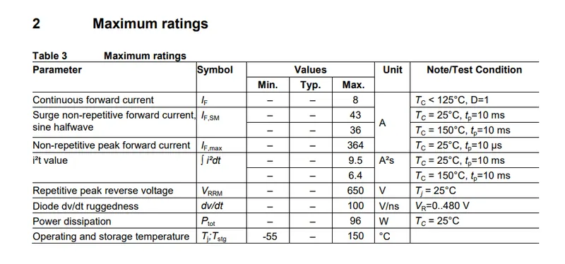
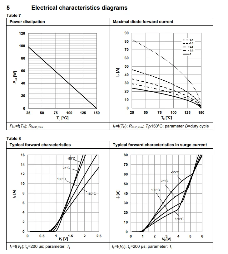
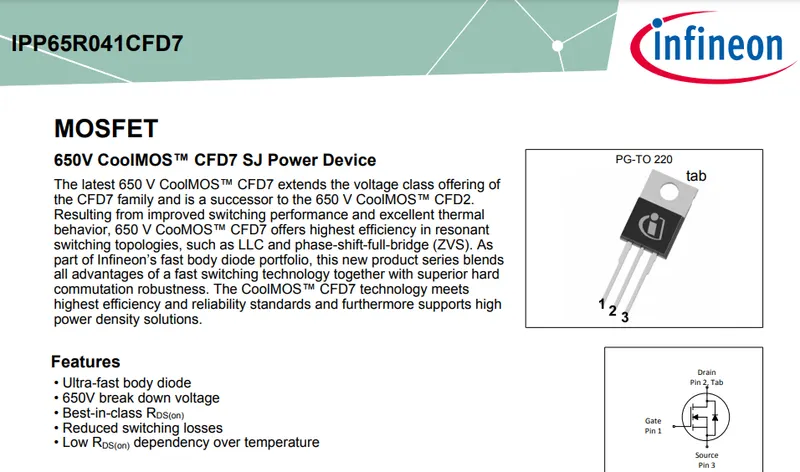
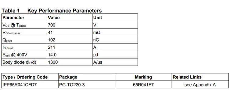
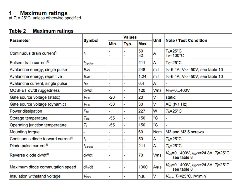
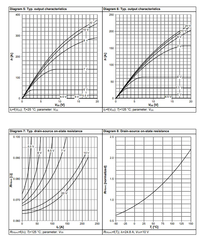
for the swtching here mosfet is selected of infineon IPP65R041CFD7
- Passive component designs including filters
load 0 to 7Amp
maximum load at 7 amp
load resistance R = 350/7 = 50ohm
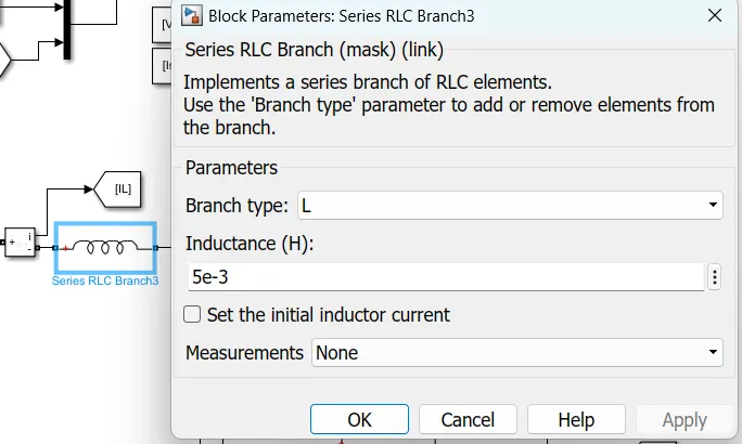
Filter inductor
for the inductor Value L = Vinpeak *k/(Fsw*dI)
here ke is duty factor
Vinpeak - peak value of rectifier output Voltage
dI - current ripple factor - 30%
L = 5e-3h
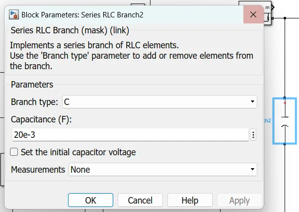
filter Capacitor
C= Iout/(2pi*fsw*dV)
Iout - out put current
dV - out put voltage ripple - 2%
C= 20E-3F
- Controller design
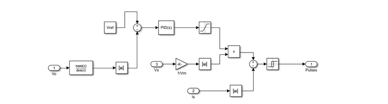
- boost converter is controlled using a close loop control with outer Voltage loop and innner current control loop
- Voltage control loop ensure adequet refrence at the output wile the current control ensure the UPF operation
- TThe reference Voltage is compared with the measure DC out put Voltage
- The error if fed to the PI controller which gives the maximume required value of the current
- Simulation results
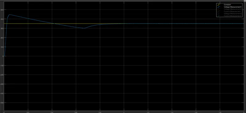
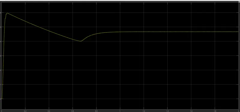
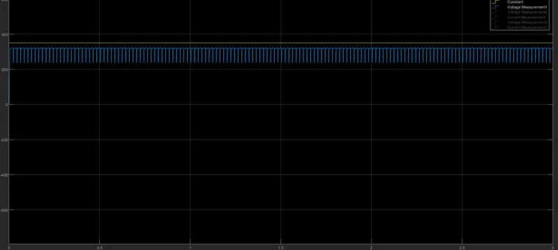
Refrence Voltage and actual output voltage
Input Voltage and Input Current
OutPut Current
- Validation with the design criterion
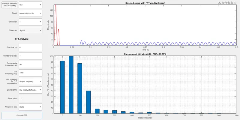
Out Put Current results
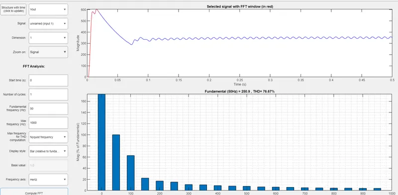
OutPut Voltage results
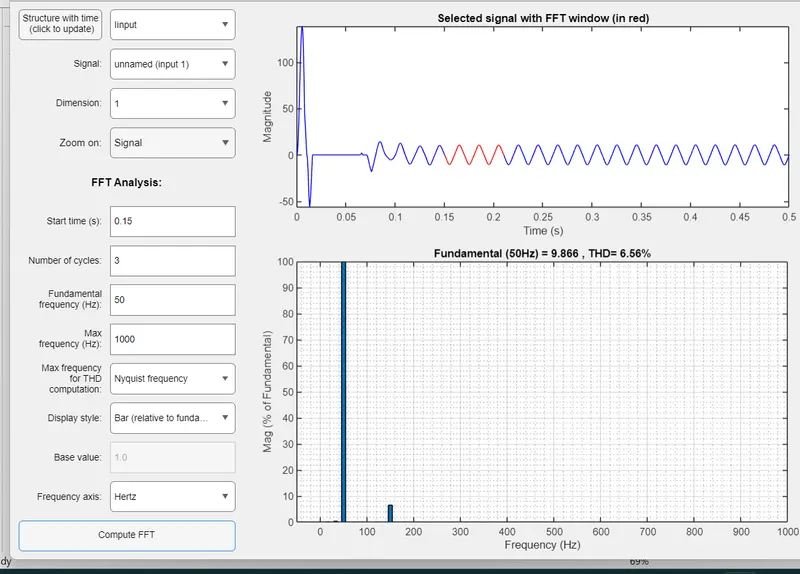
Input Current nature
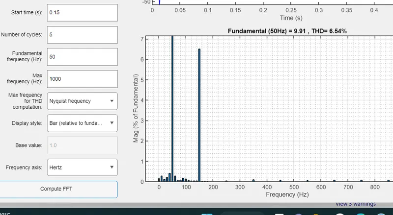
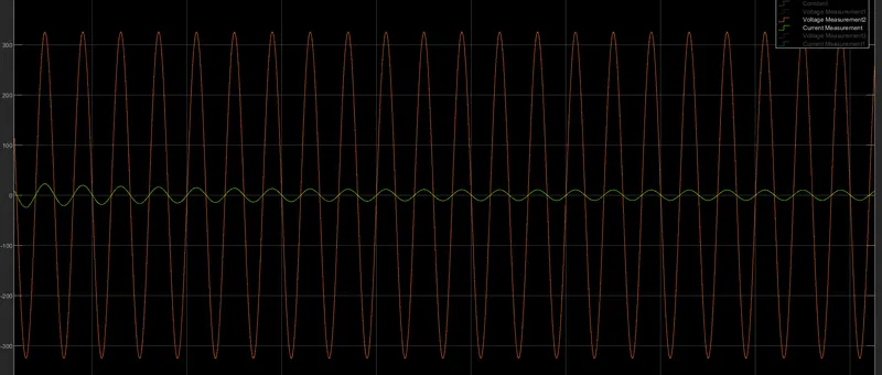
after ckt came in stable condition my total harmonic distortion came around 6% at fandamental freq of 50 Hz
this result is desirable and also pf is good near about unity
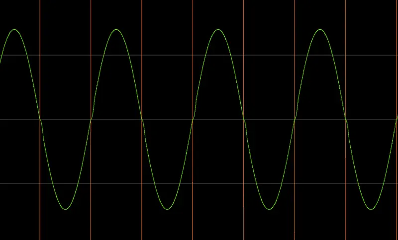
Input Voltage and Input current is in phase as you see in result
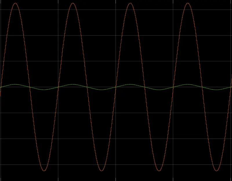
You can see that the current and voltage are close to being in phase and that the current has a general sinusoidal shape with minimal distortion.
My input Power factor
'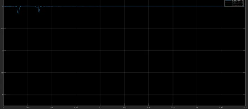
Analysis of this system indicates that the power factor is just under 0.99 and the THD is about 10%. These numbers indicate that the power quality is quite good, and they would be sufficient for meeting the harmonic current requirements of IEC 61000-3-2 as well as the power factor requirements of Energy Star 80 Plus.
- Redesign the above power supply with the PWM rectifier. Give the difference in both power supplies in terms of cost, control complexity, degrees of freedom, additional features and efficiency.
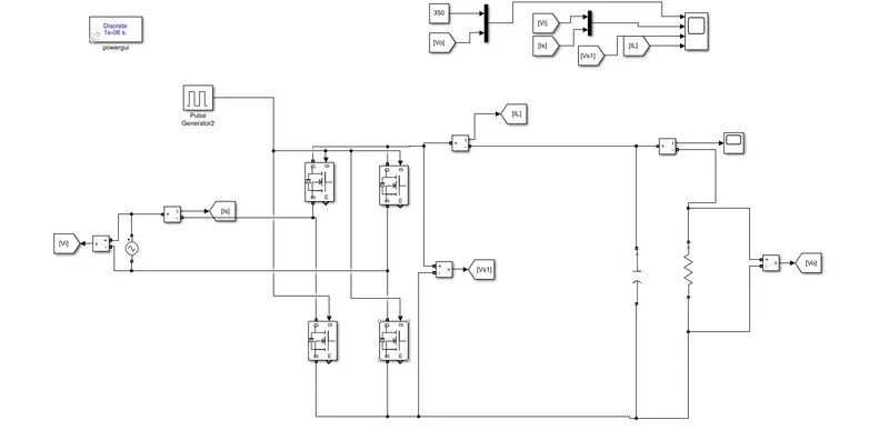
here in the both of simulation model having some major diff.
- COST - cost of the converter is very differance pwm converter is having large number of switching device
- number of swithch is so control complexiblity is also larg
- in pwm rectifier having more swtching loss due large number of switch.
Part B:
Design a high-performance high voltage DC power supply for 15 kV dc output and load in the range of 0-10A. The supply should meet the harmonic standard limits for input power quality such that current THD limits are satisfied with input power factor >0.98 value. The input side is connected to three-phase LV grid with parameters as 11kV (line-line), 50Hz.
Design the supply to give following specifications:
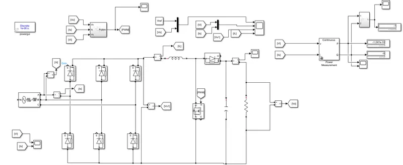
- Component selection and justification
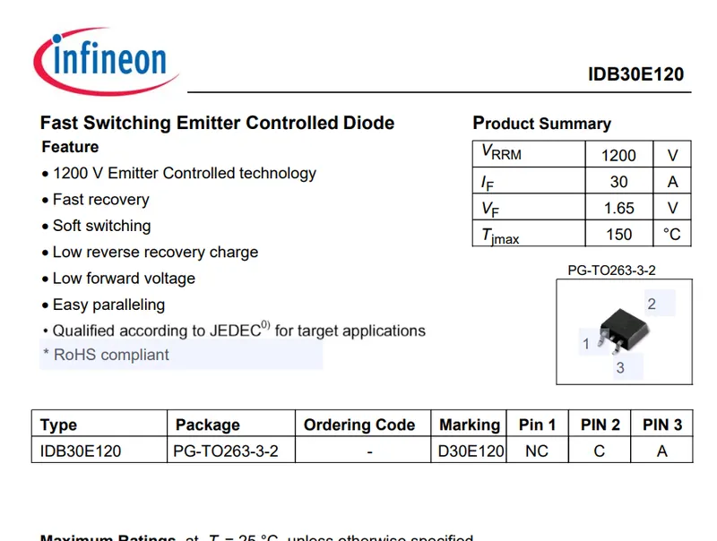
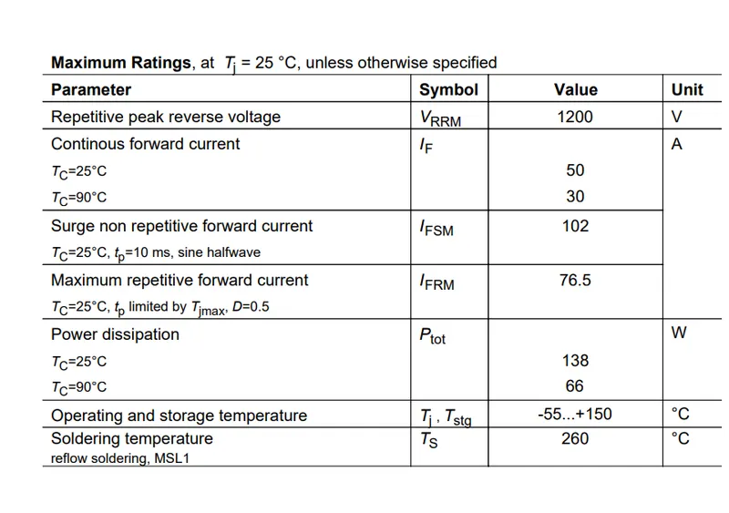
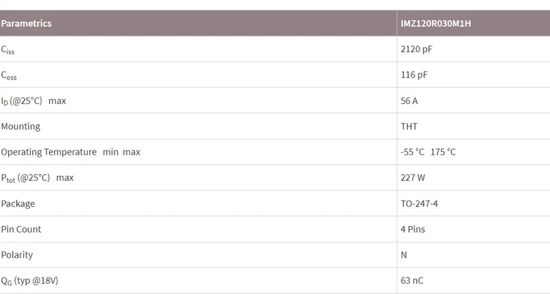
Diode- IDB30E120 is selected
this diode having 50 amp currrent carring capacity at 25 deg temp
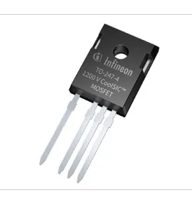
here IMZ120R030M1H of infeion mosfet is selected
this mosfet is use as a module for sufficent blocking voltage capability upto 24kv also having current capacity 56 amp that value disirable for this model

- Passive component designs including filters
load resistance R = 15000/10 = 1500 ohm ( maximum load)
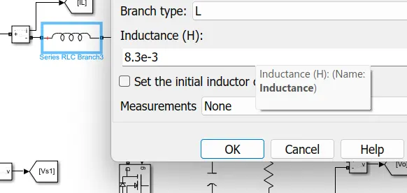
Filter Inductor
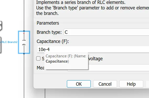
Filter Capactor
- Controller design
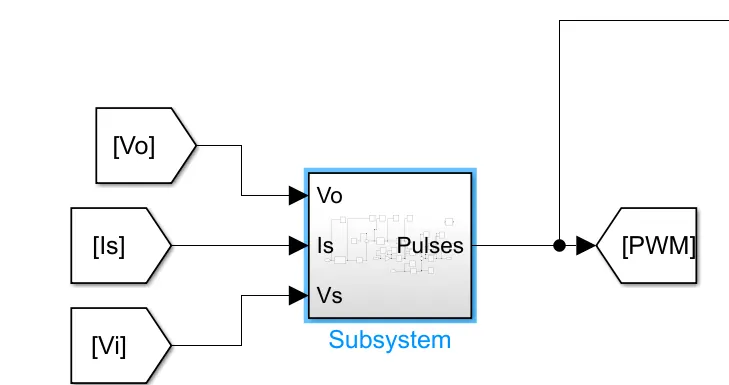
Closed-loop control is needed to ensure that the output voltage is maintained and the AC current is sinusoidal and in phase with the AC voltage. It is beyond the scope of this article to describe how the control system is designed, but Figure 6 gives you a general idea of the overall system; it shows a boost PFC circuit with a controller block that accepts four inputs and generates a pulse-width-modulated (PWM) output applied to the gate of S1.
The control system shown in Figure 6 requires three things:
- measurement of the output voltage (Vdc) to ensure that it is maintained at the reference level (Vref)
- measurement of the AC voltage to provide a reference for the inductor current
- measurement of the average inductor current to ensure that it tracks the rectified AC voltage
The control system would typically be a PI or PID control system that ensures that the difference between the reference signals and the required signals is as small as possible.
- Simulation results
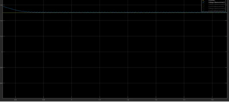
Output voltage
Input Voltage and Current
- Validation with the design criterion
pf > 0.99
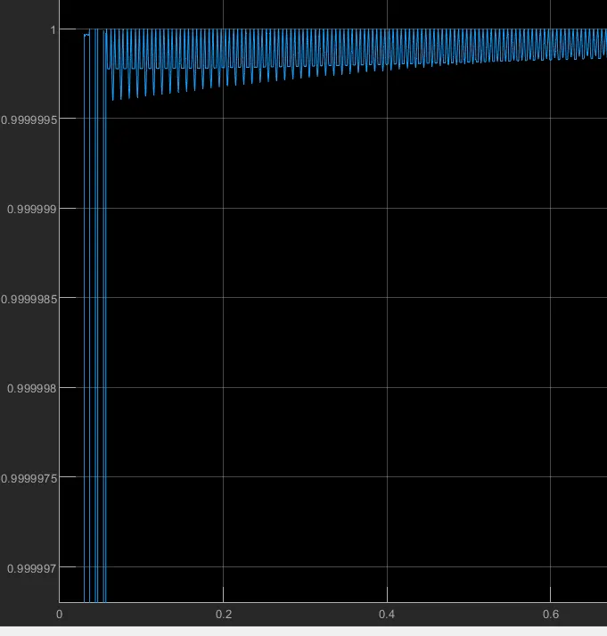
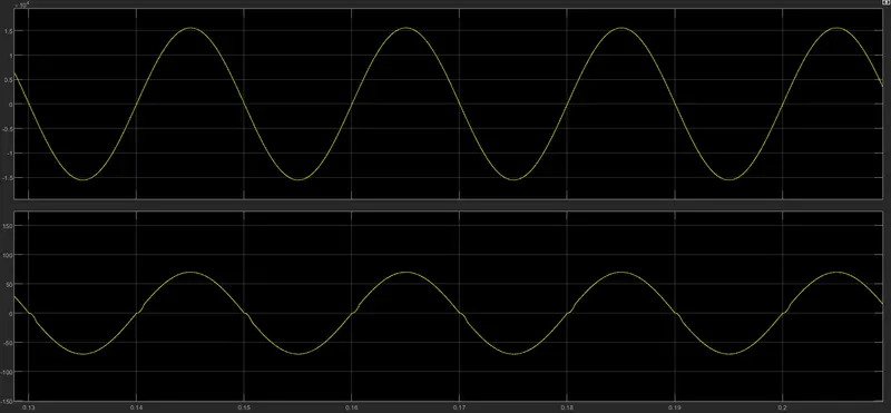
as you see here input voltage and current both are in same phase with minimum distortion , power factor 0.99 and THD 6.54% that meanse power quality is good .