Design of Isolated interleaved forward converter
Selected 1 st Project
Given Data:
Input Voltage,Vin = 45 to 60 V
Output Voltage,Vo = 3 V
Ouput Current, Iout = 100 Amps
Assumed Switching frequency fs = 500 kHz
Requirements:
1) Need to Design Isolated interleaved DC-DC Converter for efficiency greater than 85 %
2) Simulate and need to show the input voltage, the output voltage, the input current, the output current, the system efficiency and any other simulation plots necessary to evaluate design.
Solution:
For this input requirement i am choosing Isolated interleaved forward converter toplogy.
A two phase interleaved forward converter is just simply two forward converters operating 180 degrees out of phase. The two key benefits of interleaving are reduced input and output capacitor ripple currents as compared to a standard forward converter.
Step 1: Transformer Turns Ratio:
The first step is to calculate the required transformer turns ratio required for the design. The winding ratio between the primary winding (Np) and the reset winding (Nr) is often chosen as 1 The following equations are used to calculated the approximate transformer turns ratio with a maximum duty cycle of 0.5 at minimum input voltage (Vin(min)).
The Winding ratio between primary (Np) and secondary winding (Ns) must be small enough to ensure th required output voltage can be achieved at maximum D i.e 0.5 and mimimum input voltage.
Transformer Ratio (a) = Np/Ns = [(Vin-1) / (vo +1)]*Dmax
a = [(45-1)/(3+1)]*0.5
a = 5.5
Step 2: Output inductors Selection:
The output inductor was sized based on the worst case ripple current that occurs at minimum duty cycle, Dmin, and a maximum output power. The output capacitor ripple current cancellation of interleaving two forward converters allowed the output inductors Lout to be designed for a ripple current that was roughly 60% of the maximum load current.
Dmin = a*[(Vout+1)/(Vin(max)-1)]
Dmin = 5.5*[(3+1)/(60-1)]
~= 0.35
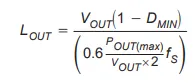
from above fomula
Lout = [3*(1-0.35)]/[0.6*(300/(3*2))*500kHz]
= 130 nH
Take Lout = 150 nH
Step 3: Selection of semiconductor devices
Before selecting electrical components for output diodes and FETs a power budget needs to be set for each component, to ensure that the efficiency goal (η) of 85% can be achieved. To achieve this design goal a power budget was set for each semiconductor device to dissipate less than one sixth the maximum allowable losses.
Psemi < Pout(max)[(1-η)/6]
< 300*[(1-0.85)/6]
< 7.5W
Each semiconductor device should be less than 7.5W to achieve efficiency goal.
i) Forward Mosfet Selection:
The Mosfet is to be selected by considering following parameters
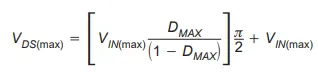
Vds ~= 160 V
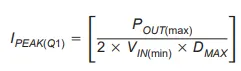
I peak = [300/(2*45*0.5)]
I peak = 5 Amps
While selecting the MOSFETs the above parameters need to taken into considaration and total losses from MOSFETs not more than 7.5 W.
ii) Diodes Selection:
The power budget that is remaining for the output rectifier selection is roughly 30W (45W - 15W). The following equations will estimate the maximum reverse voltage on the output rectifiers, VD(max), and the maximum power dissipated by all the diodes combined PD(max). The diodes used in this design had roughly 0.3V forward voltage drop.
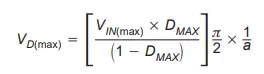
Vd(max) = 17.13 V
Vd(max) ~= 20 V
Pdmax = (Pout*Vf)/Vout
= (300*0.3)/3
Pdmax = 30W
While selectining diodes need to consider above parameters.
Step 4: Output Capacitor Selection:
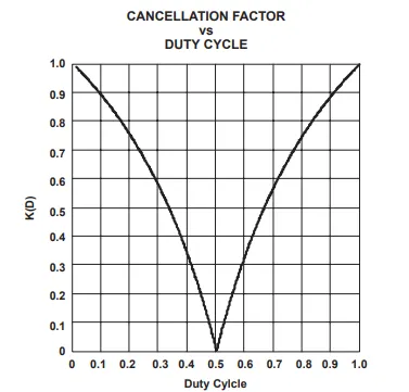
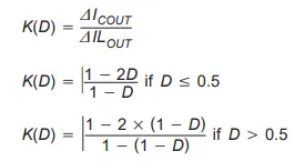
The capacitor needs to be selected to meet an output voltage ripple requirement that is dependent on the amount of ac inductor ripple current that needs to be filtered. It is required that the worst case output capacitor current to be calculated. from the below graph (from Texas instrument application note) and the following calculations we can find how the ratio of capacitor ripple current and inductor ripple current vary with D. In this design the duty cycle varies from 0.35 to 0.5.
we know
Delta(ILout) = 60% IL/2
= 0.6*100/2
= 30 Amps
then K(D) = (1-2*0.35)/(1-0.35)
= 0.461
Then Delta(ICout) = 0.461*30
Delta(ICout) = 13.83 Amps
Maximum allowable ESR value to select Capacitor to meet efficiency goal is
ESR( Cout) < (Vripple*0.4) / Delta(ICout)
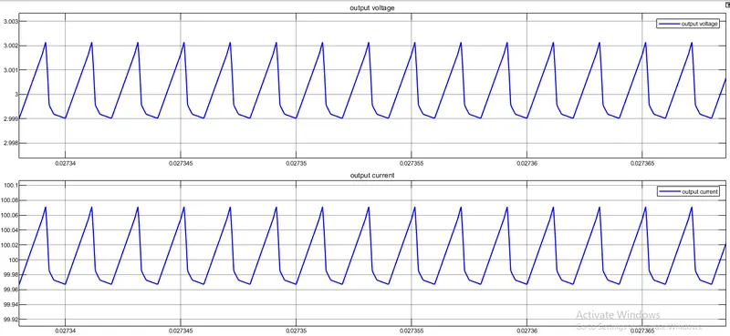
Assume allowable output voltage ripple is 2% of Vo
= 0.06V
ESR = (0.06*0.4)/13.83
ESR(Cout) should be less than 1.7 mohm.
Cout = [Delta(ICout)*Dmin] / [8 *Vripple*0.1*fs]
Cout = 201.6 uF
Take Cout = 220uF
Step 5 :Input Capacitor Selection:
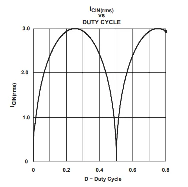
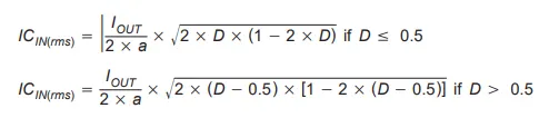
It is dependent on ripple voltage requirements and capacitor ripple current. The first step is to calculate the worst case capacitor ripple current. The following equations and Figure ( From Texas instrument Application Note) show how the input capacitor RMS current (ICin(rms)) varies with duty cycle. In this design D varies from 0.35 to 0.5, from the graph it can be observed that the worst case input ripple current occurs at a duty cycle of 35%.
from above formulas
we can calculate
ICin = 4.17 Amps
The following equations were used to select the minimum input capacitance (CIN) and the maximum allowable ESRCin for the design. VRIPPLE(in) is the input voltage ripple requirement which was 3% of the minimum input voltage VIN(min).
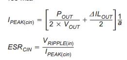
The peak input capacitor current, IPEAK(cin), for this design was roughly 11.8 A and the maximum allowable ESR for the design was roughly 114 mΩ.
To select the minimum input capacitance requires calculating the duty cycle ratio D where the RMS current is at its peak. For this design the largest amount of ripple current occurs at D of 0.35.
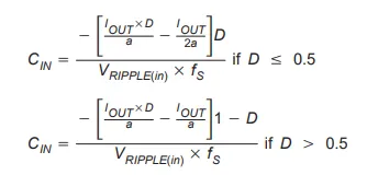
As D < 0.5 used first formula to fin Cin
Cin = 1.5 uF
Take Cin = 2 uF.
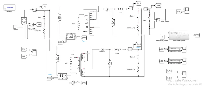
Step 6: Simulation of above design in Simulink
With all above calculated values designed interleved forward converter Toplology as shown below.
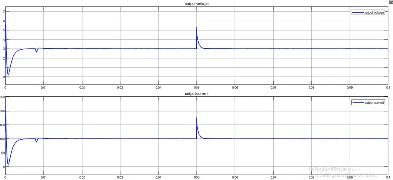
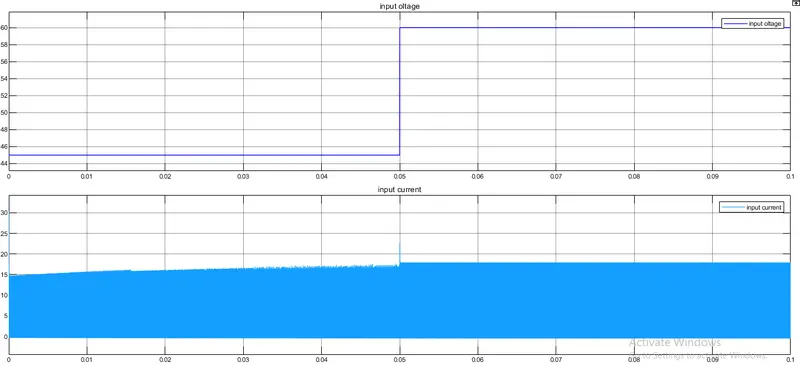
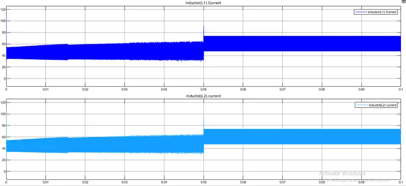
To get the output voltage responce with change in input voltage used step signal and the input voltage is changed from 45V to 60V at time of 0.05 sec.
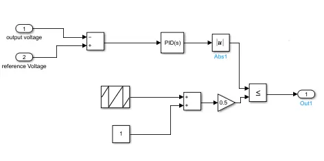
Feedback System:
Step 7: Verification of Required Waveforms:
1)Output Voltage and Output Current:
Zoom out Mode:
Zoomin Mode:
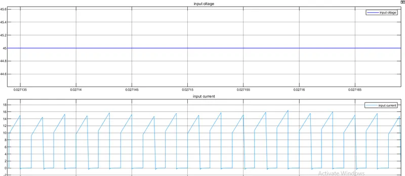
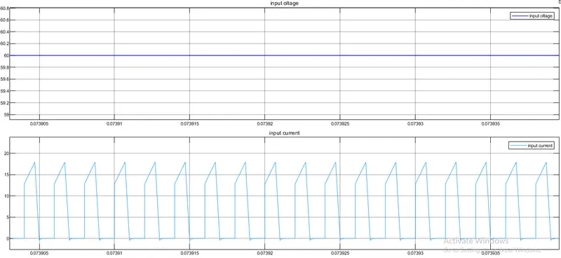
2)Input Voltage and Current:
Zoomout Mode:
Zoomin Mode:
For Time T< 0.05 Sec
For T > 0.05 Sec
3)Inductor Currents:
Zoomout Mode:
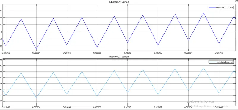
Zoomin Mode:
For T < 0.05 Sec
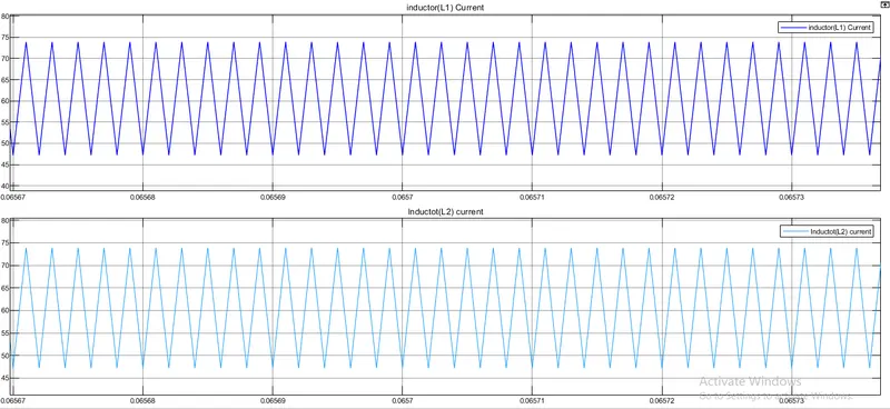
For T > 0.05 Sec
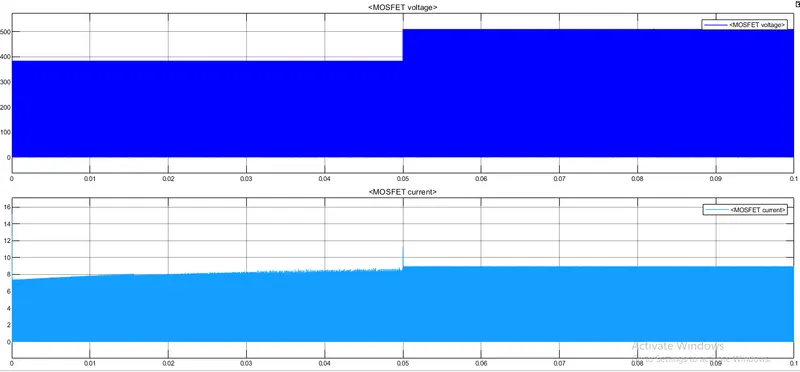
4)MOSFET -1 Voltage and Current:
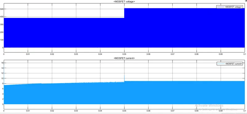
5)MOSFET -2 Voltage and Current:
Conclusion:
Designed an interleaving DC/DC forward converter system for a data centre application with given specification and all required output wave forms like output voltage and current, input voltage and current and so on are simulated in simulink and shown above the simulink file is also attached.