Design of Non-Isolated CCM converters
The following three toplogies are selected for my project.
1) S.no: 5) Sepic CCM input voltage = (30 to 60 V) outputvoltage = 45 V power = 1 kW
2) S.no: 10) Buck CCM input voltage = 400 to 500 V output voltage = 300 V power = 5 kW
3) S.no: 12) Buck Boost CCM input voltage = 300 to 600 V output voltage = -450V power = 2 kW
Topology-1:
SEPIC CCM :
Givendata:
input voltage Vin = 30 - 60 V
output voltage Vout = 45 V
power P = 1 kW
Assume Switching Frequency fs = 500 kHz
Solution:
Load Resistance R = V^2 / P
= 2.025 ohm
i) Design of Converter Inductors and Capacitors:
a) Converter Duty Ratio:
V0 / Vin = D/(1-D)
For Vin = 30V
45/30 = D / (1-D)
D = 0.6
For Vin = 60V
45/60 = D / (1-D)
D = 0.43
b) Conveter Inductors :
Here i designed inductors for maximum of 5% Ripple current.
We know for Sepic Converter input side Inductor (L1) current is
IL1 = p/Vin = 1000/60 = 16.667 Amps ( To obtain minimum amount of ripple current take Vin = 60 )
Ripple Current Delta(IL1) = 5% of 16.667 A
= 0.833 A
Inductor L1 = (Vin/fs*Delta(IL1)) * D
Caluculting Inductor value for worst condition so take D = 0.6 and Vin 60V
L1 = (60 / ( 500k * 0.833)) * 0.6
= 86.43 uH
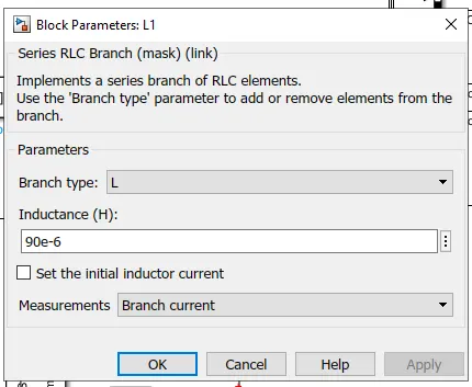
Take L1 = 90 uH
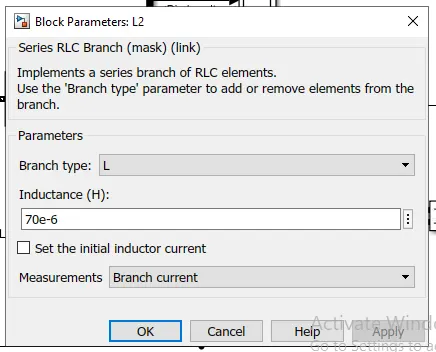
Sepic Converter output side Inductor (L2) current is
IL2 = p/Vo = 1000/45 = 22.22 Amps
Ripple Current Delta(IL2) = 5% of 22.22 A
= 1.111 A
Inductor L2 = (Vin/fs*Delta(IL2)) * D
Caluculting Inductor value for worst condition so take D = 0.6 and Vin 60V
L2 = (60 / ( 500k * 1.111)) * 0.6
= 64.80 uH
Take L2 = 70 uH
Intermidiate Capacitor(C1):
we know for Sepic converter C1 = VoD/(R*fs*Delta(Vc1))
Delta(Vc1) = Vin = 30V
Assume 1% voltage Ripple
then Delta(Vc1) = 0.01* 30 = 0.3
C1 = (45*0.6) / (2.025*500k*0.3)
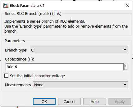
C1 = 88.88 uF
Take C1 = 90 uF
Output Capacitor(C2):
we know for Sepic converter C2 = D/(R*fs*(Delta(Vo)/Vo)
Assume 1% output voltage Ripple required
C2 = (0.6) / (2.025*500k*0.01)
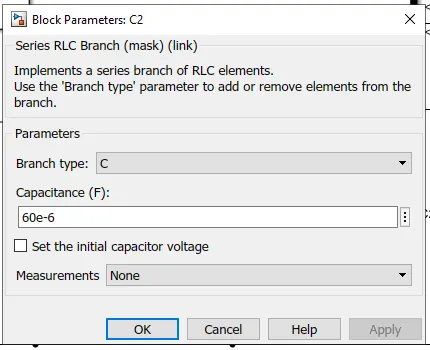
C2 = 54.42 uF
Take C2 = 60 uF
ii) Full Schematics of Converter:
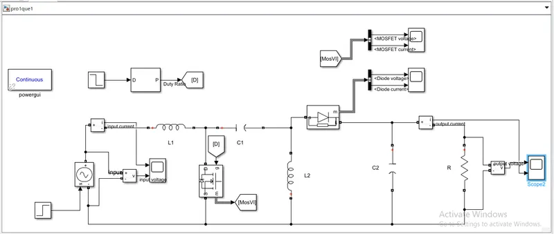
iii) Required Waveforms to show system ability to track output voltage and mosfet & Waveforms:
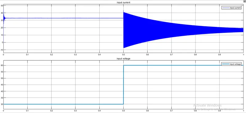
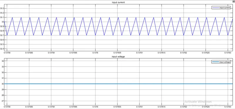
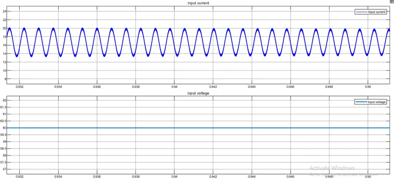
Input Voltage and Input current:
Here input voltage changed from 30V to 60V at 0.5 sec to monitor output voltage responce.
Zoomout Mode:
Zoomin Mode:
at < 0.5 Sec.
at > 0.5 Sec
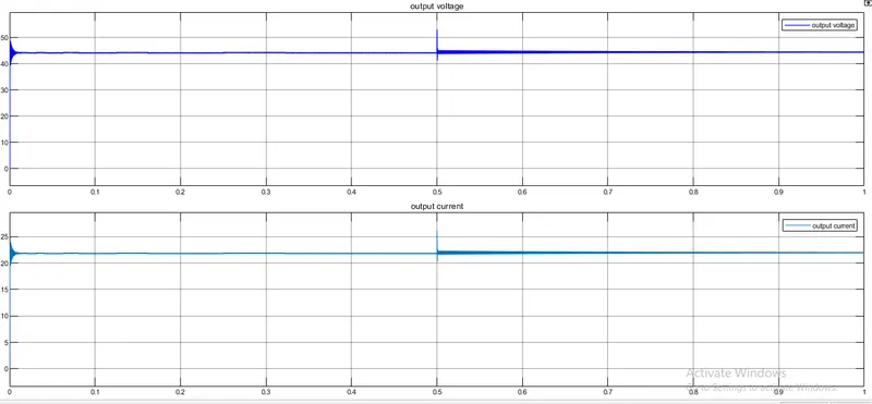
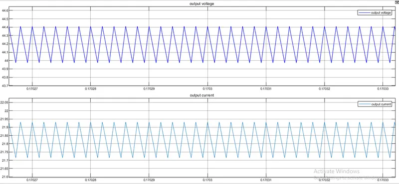
Output Voltage and Current Waveforms:
Zoomout mode:
Zoomin Mode:
fot time < 0.5 Sec
for time > 0.5 Sec
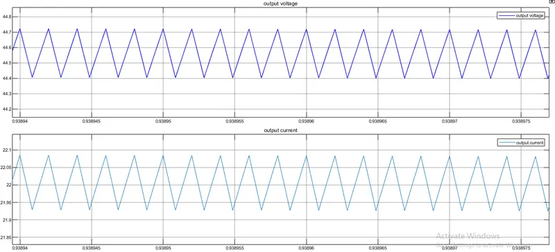
With the above waveforms we can say that after changing the input voltage from 30 V to 60 Volts at 0.5 sec the output voltage track the required voltage of 45 V.
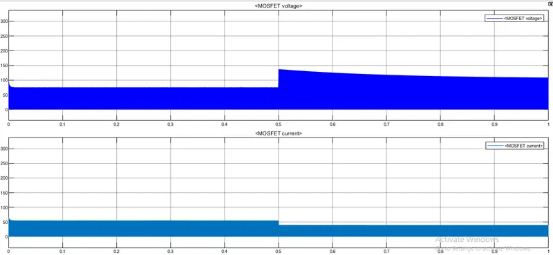
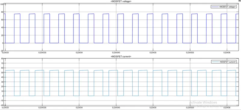
Mosfet Voltage and Current Waveforms:
Zoomout MOde:
Zoomin Mode:
for time < 0.5 Sec
for time > 0.5 Sec
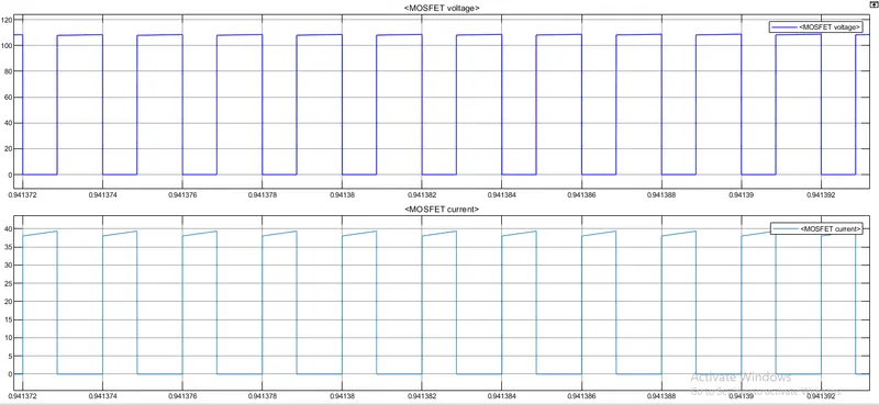
With reference to the above waveforms we can say maximum voltage across MOSFET is 110 V and Maximum current through MOSFET is 60 Amps.
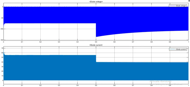
Diode Voltage and Current Waveforms:
Zoomout Mode:
Zoomin Mode:
for time < 0.5 Sec
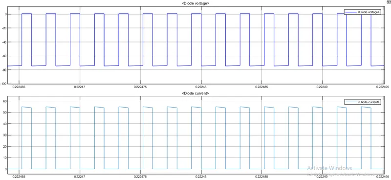
For time> 0.5 Sec
Zoomin MOde:
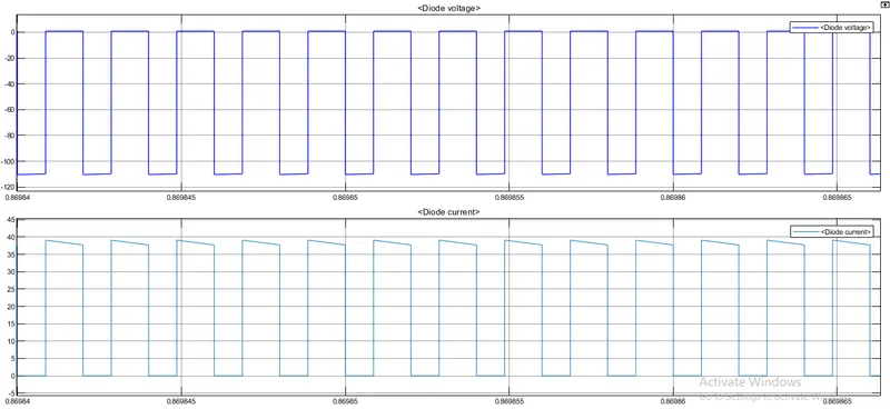
With reference to the above waveforms we can say maximum voltage across Diode is 110 V and Maximum current through Diode is 60 Amps.
iv) Specification of components used in this model:
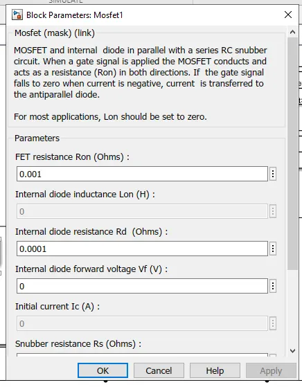
MOSFET:
Vds = 110V
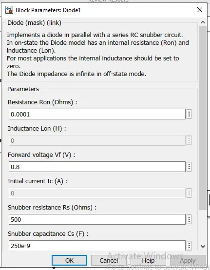
Diode:
Vd = 110 V
Inductor L1:
Inductor L2:
Capacitor C1:
Capacitor C2:
Conclusion:
The Given Toplology is successfully execucted with required components and with model requirements, full schematic of converter shown and executed sucessfully in simulink with all nessesary waveforms and proved system is tracking required output voltage with dynamic change in input voltage,and also the required specifications used to design this topology are shown above.
Topology-2:
BUCK CCM :
Givendata:
input voltage Vin = 400 - 500 V
output voltage Vout = 300 V
power P = 5 kW
Assume Switching Frequency fs = 500 kHz
Solution:
Load Resistance R = V^2 / P
= 18 ohm
i) Design of Converter Inductor and Capacitor:
a) Converter Duty Ratio:
V0 / Vin = D
For Vin = 400V
300/400 = D
D = 0.75
For Vin = 500V
300/500 = D
D = 0.6
b) Conveter Inductors :
Here i designed inductor for maximum of 5% Ripple current.
i.e IL = Vo/R = 300/18 = 16.67 Amps
Delta(IL) = 0.8335 Amps
We know for Buck Converter
Inductor L = (Vout/fs*Delta(IL)) *(1-D)
Calculating Inductor value for worst condition so take D = 0.6
L = (300 / ( 500k * 0.8335)) *( 1-0.6)
= 287 uH
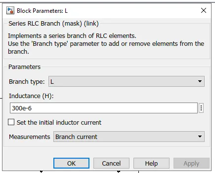
Take L = 300 uH
Output Capacitor(C):
we know for Sepic converter C = (1-D)/(8*L**fs^2*(Delta(Vo)/Vo)
Assume 1% output voltage Ripple required
C = (1-0.6) / (8*287u*500k*500k*0.01)
C = 69.686 nF
Take C = 100 nF
ii) Full Schematics of Converter:
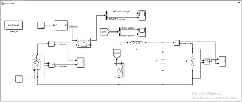
iii) Required Waveforms to show system ability to track output voltage and mosfet & Waveforms:
Input Voltage and Input current:
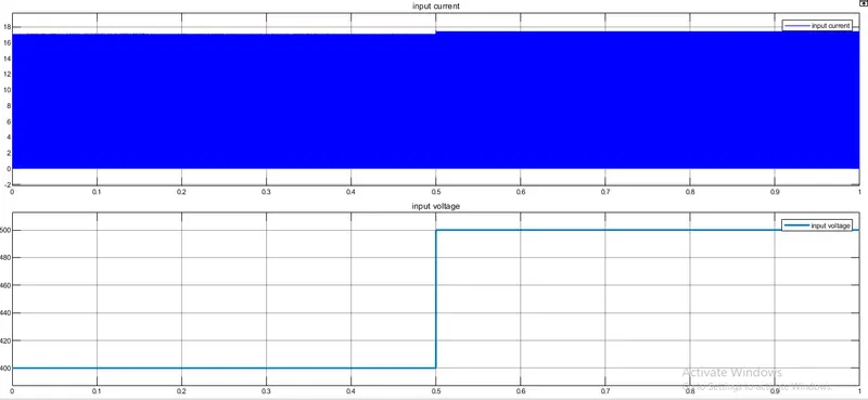
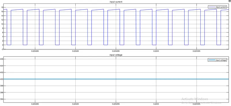
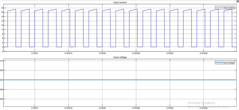
Here input voltage changed from 400V to 500V at 0.5 sec to monitor output voltage responce.
Zoomout Mode:
Zoomin Mode:
at time < 0.5 Sec.
at time > 0.5 Sec
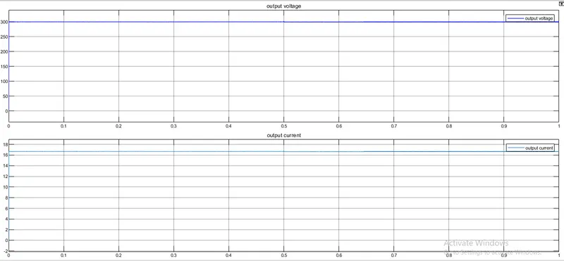
Output Voltage and Current Waveforms:
Zoomout mode:
Zoomin Mode:
fot time < 0.5 Sec
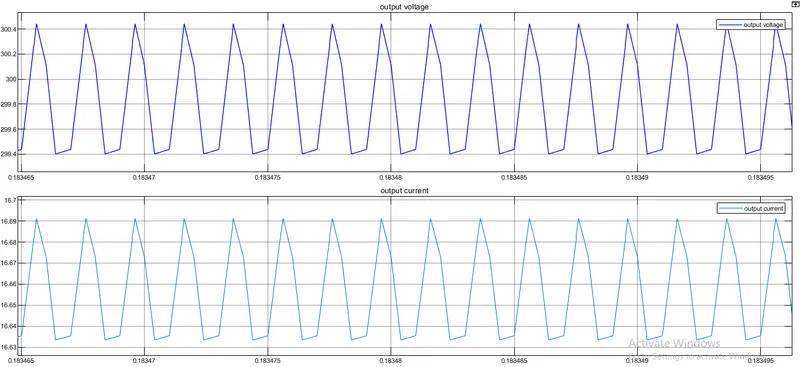
for time > 0.5 Sec
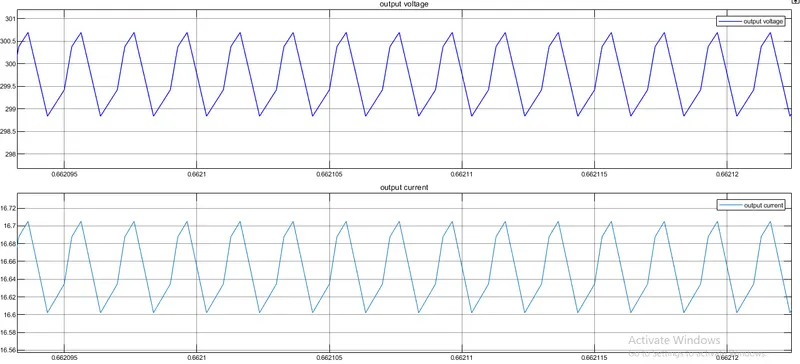
With the above waveforms we can say that after changing the input voltage from 400 V to 500 Volts at 0.5 sec the output voltage track the required voltage of 300 V.
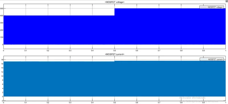
Mosfet Voltage and Current Waveforms:
Zoomout MOde:
Zoomin Mode:
for time < 0.5 Sec
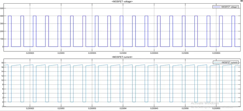
for time > 0.5 Sec
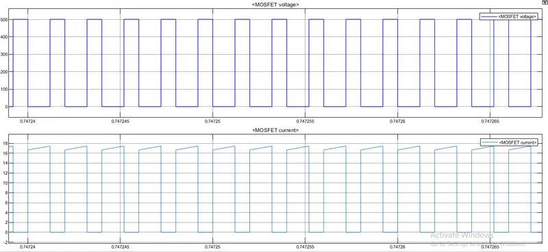
With reference to the above waveforms we can say maximum voltage across MOSFET is 500 V and Maximum current through MOSFET is 18 Amps.
Diode Voltage and Current Waveforms:
Zoomout Mode:
Zoomin Mode:
for time < 0.5 Sec
For time> 0.5 Sec
Zoomin Mode:
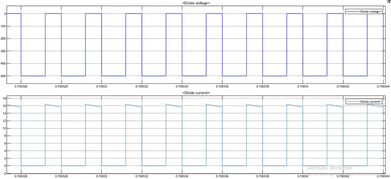
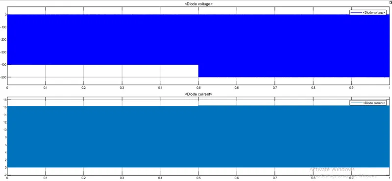
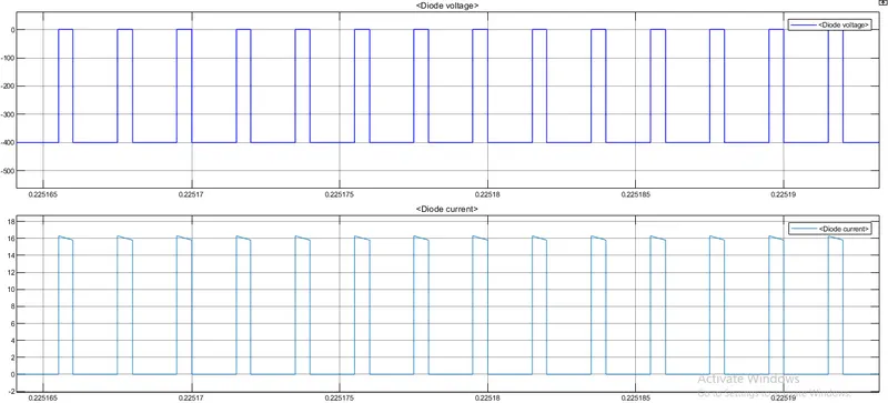
With reference to the above waveforms we can say maximum voltage across Diode is 500 V and Maximum current through Diode is 17 Amps.
iv) Specification of components used in this model:
MOSFET:
Vds = 500V
Diode:
Vd = 500 V
Inductor L:
Capacitor C:
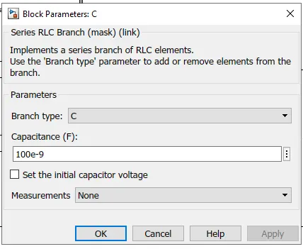
Conclusion:
The Given Toplology is successfully execucted with required components and with model requirements, full schematic of converter shown and executed sucessfully in simulink with all nessesary waveforms and proved system is tracking required output voltage with dynamic change in input voltage,and also the required specifications used to design this topology are shown above.
Topology-3:
BUCK - BOOST CCM :
Givendata:
input voltage Vin = 300 - 600 V
output voltage Vout = -450 V
power P = 2 kW
Assume Switching Frequency fs = 500 kHz
Solution:
Load Resistance R = V^2 / P
= 101.25 ohm
i) Design of Converter Inductor and Capacitor:
a) Converter Duty Ratio:
V0 / Vin = -D/(1-D)
For Vin = 300V
-450/300 = -D/(1-D)
D = 0.6
For Vin = 600V
-450/600 = -D/(1-D)
D = 0.43
b) Conveter Inductors :
Here i designed inductor for maximum of 5% Ripple current.
i.e IL = Vo/R = 4.44 Amps
Delta(IL) = 0.222 Amps
We know for Buck Converter
Inductor L = (Vout/fs*Delta(IL)) *(1-D)
Calculating Inductor value for worst condition so take D = 0.43
L = (450 / ( 500k * 0.222)) *( 1-0.43)
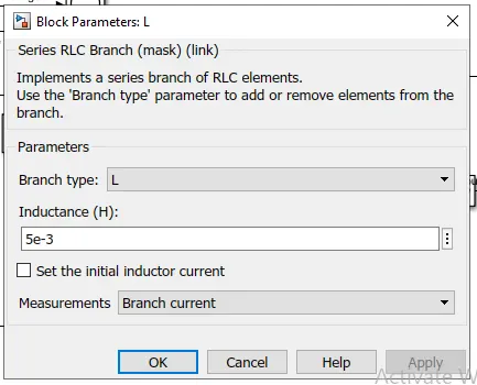
= 2.31 mH
Take L = 5 mH
Output Capacitor(C):
we know for Sepic converter C = (D)/(R*fs*(Delta(Vo)/Vo)
Assume 1% output voltage Ripple required
C = (0.6) / (101.25*500k*0.01)
C = 1.185 uF
Take C = 2 uF
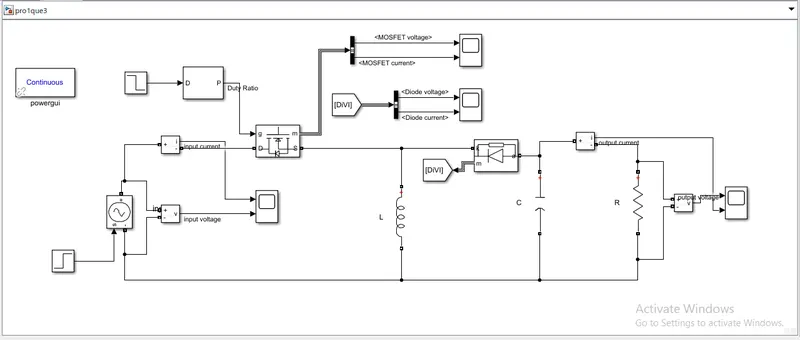
ii) Full Schematics of Converter:
iii) Required Waveforms to show system ability to track output voltage and mosfet & Waveforms:
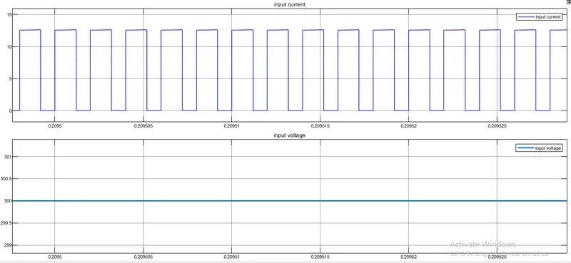
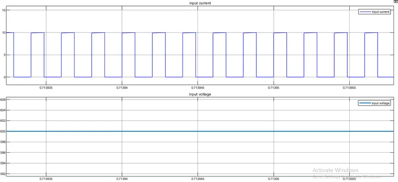
Input Voltage and Input current:
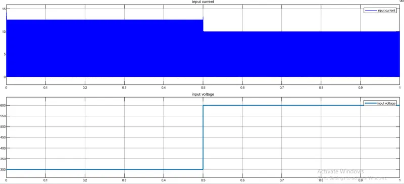
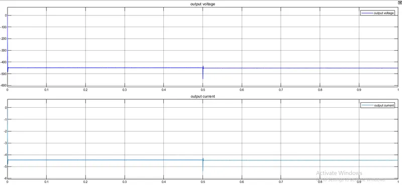
Here input voltage changed from 300V to 600V at 0.5 sec to monitor output voltage responce.
Zoomout Mode:
Zoomin Mode:
at time < 0.5 Sec.
at time > 0.5 Sec
Output Voltage and Current Waveforms:
Zoomout mode:
Zoomin Mode:
fot time < 0.5 Sec
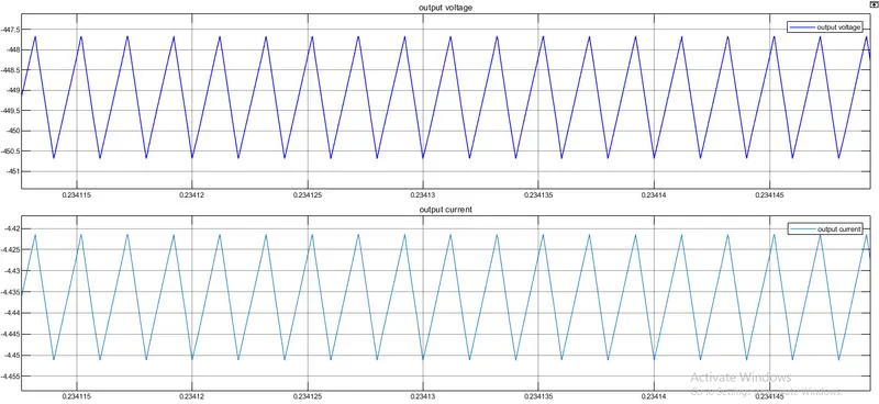
for time > 0.5 Sec
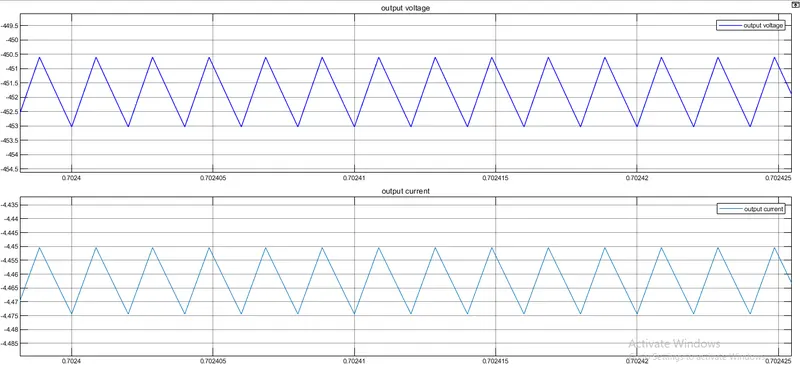
With the above waveforms we can say that after changing the input voltage from 300 V to 600 Volts at 0.5 sec the output voltage track the required voltage of -450 V.
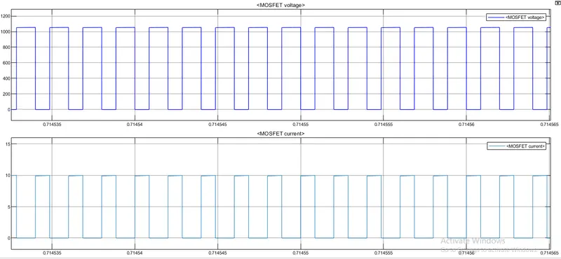
Mosfet Voltage and Current Waveforms:
Zoomout MOde:
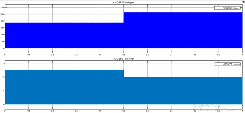
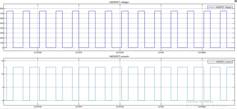
Zoomin Mode:
for time < 0.5 Sec
for time > 0.5 Sec
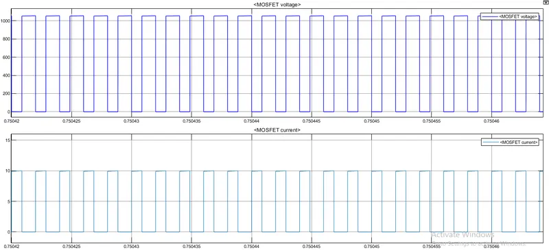
With reference to the above waveforms we can say maximum voltage across MOSFET is 1050 V and Maximum current through MOSFET is 13 Amps.
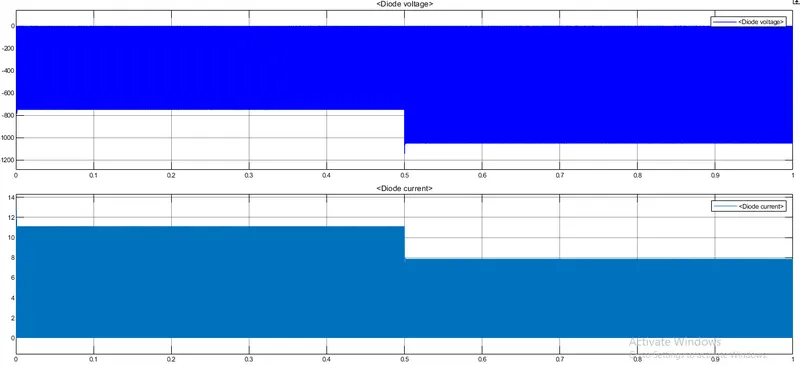
Diode Voltage and Current Waveforms:
Zoomout Mode:
Zoomin Mode:
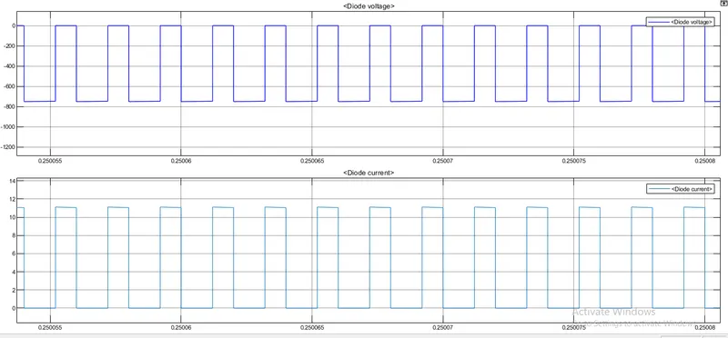
for time < 0.5 Sec
For time> 0.5 Sec
Zoomin Mode:
With reference to the above waveforms we can say maximum voltage across Diode is 1050 V and Maximum current through Diode is 13 Amps.
iv) Specification of components used in this model:
MOSFET:
Vds = 1050V
Diode:
Vd = 1050 V
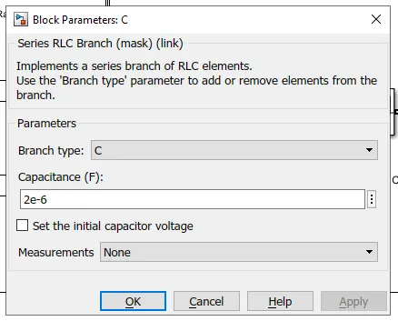
Inductor L:
Capacitor C:
Note: for simulation purpose for all capacities i used Mosfets for swithing purpose as we know for high voltages Mosfets are not preferable and need to replace with IGBTs please make a note of it.
Conclusion:
The Given Toplology is successfully execucted with required components and with model requirements, full schematic of converter shown and executed sucessfully in simulink with all nessesary waveforms and proved system is tracking required output voltage with dynamic change in input voltage,and also the required specifications used to design this topology are shown above.