Project 1- Traffic Jam Assistant Feature
AIM
- Model Development of a single feature of Traffic Jam Assist using MATLAB & Simulink as well as Code Generation using Embedded Coder.
OBJECTIVES
- Model Development as per MBD guidelines. Creation of Simulink Data Dictionary.
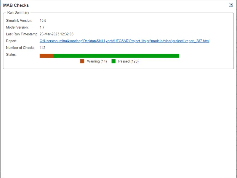
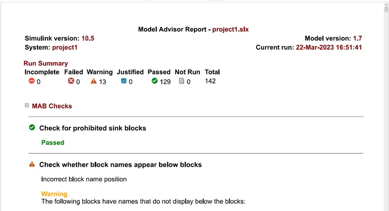
- Code Generation using Embedded Coder Generating Model Advisor ReporT
Step:-1
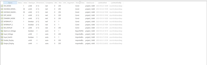
Data Dictionary creation: (TrafficJamAssistant.sled)
- A new Simulink data dictionary is created and updated signals & calibration Data List as per our requirements.
- The very first thing that we will do is create a Simulink Data Dictionary using the given Signal and Calibration Data List.
The following is the SLDD file :
Step_2
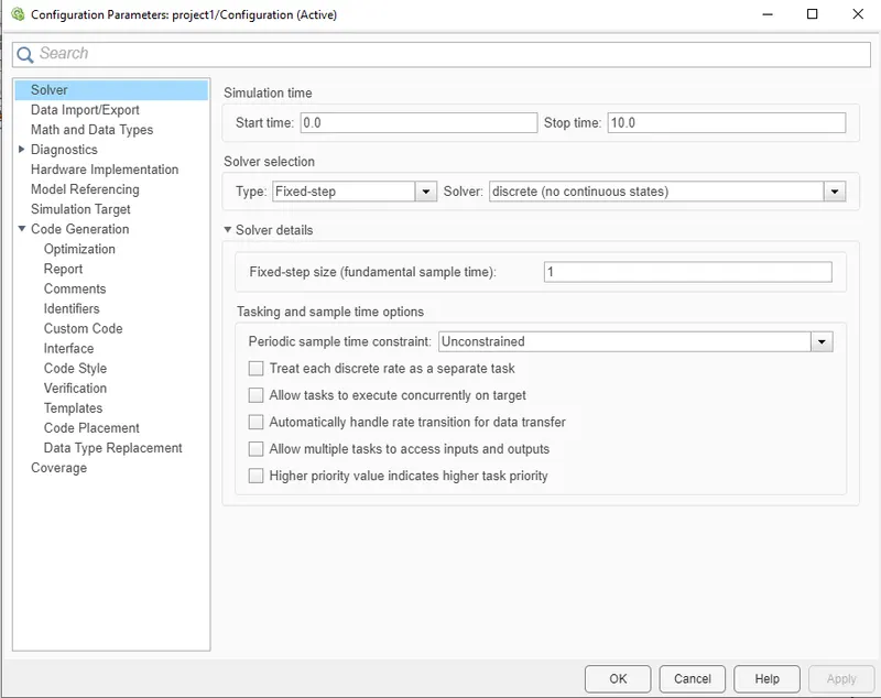
Solver configuration parameter:
- Solver type: Fixed
- Solver: discrete (no continuous states)
- Sample time: 1
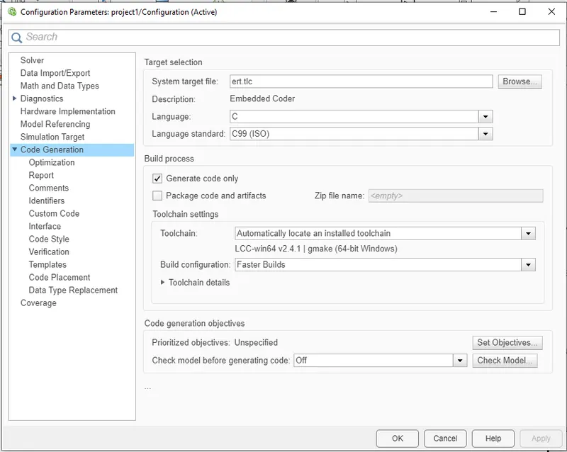
Code generation Parameters:
- System target file: ert.tlc ( Embedded Coder)
Step-3
Now we create our Simulink model
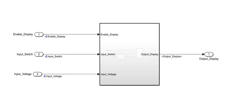
as per Requirement-1
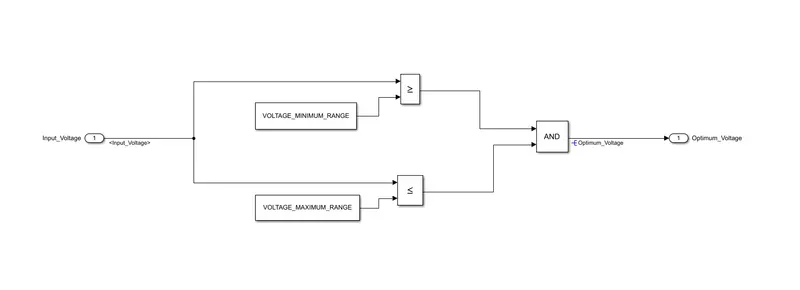
- Input Signal “Input_Voltage” is compared against voltage values “VOLTAGE_MINIMUM_RANGE” & “VOLTAGE_MAXIMUM_RANGE”.
- Incoming input signal “Input_Voltage” must be greater than – equal to “VOLTAGE_MINIMUM_RANGE” and less than – equal to “VOLTAGE_MAXIMUM_RANGE”.
- Output signal from here is “Optimum_Voltage” which will be one of the inputs to the subsystem “DisplayUnit”
As per requirement-2
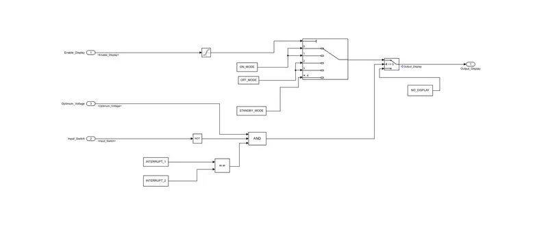
- Input Signals are “Optimum_Voltage”, “Input_Switch”,“Enable_Display”. Signal “Enable_Display” must be saturated between the range 0 – 7. Output signal from the subsystem is “Output_Display”.
- Input Signal “Enable_Display” is compared against pre – defined set of values in a multiport switch. Total data ports in the multiport switch is 5.
- Multiport switch inputs 1 & 2 is connected to calibration signal “ON_MODE”, Multiport switch inputs 3 & 4 is connected to calibration signal “OFF_MODE” while Multiport switch input 5 is connected to calibration signal “STANDBY_MODE”.
- The output from Multiport switch is connected to the first input port of the Switch block. The third input port of the Switch block is connected to the calibration signal “NO_DISPLAY”.
- Meanwhile NOT value of input signal “Input_Switch” is compared in an AND gate against input signal “Optimum_Voltage” and the output from comparing if calibration signals “INTERRUPT_1” & “INTERRUPT_2” are equal. The output of the AND gate is the second input of the switch block.
- The output from the switch block is “Output_Display”.
Code Generation:
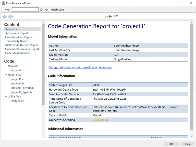
Model advisor report