Project 1- Traffic Jam Assistant Feature
Project 1- Traffic Jam Assistant Feature
Introduction to the Feature:
Traffic Jam Assistant is one of the most common feature in Advanced Driver Assistance System. Traffic Jam Assistant helps the driver arrive more relaxed at their destination, even in dense traffic or in traffic jams. As a partially automated comfort function, the system takes over the longitudinal & lateral guidance of the vehicle. This means that the car can drive off, accelerate & brake automatically, as well as steer the vehicle within certain constraints. The driver has to permanently supervise the system & be ready to take over the complete control of the vehicle at any time.

Traffic Jam Assistant system helps to avoid rear end collisions in dense traffic conditions & traffic jams. In Traffic jams, the vehicle takes over driving off, acceleration, braking and steering within same lane.
Basic Working Principle:
Traffic Jam Assistant is based on the sensors and the functionality of the Adaptive Cruise Control (ACC) with stop & go and Lane Keeping Support (LKS). When ACC ‘Stop & Go’ is turned ON, the Traffic Jam Assistant continuously analyses the speed of the surrounding vehicles and compares it with the own driving speed. If the system detects dense traffic or a traffic jam at speeds less than 60 kmph, the driver can activate the functionality by press of a button. The vehicle will now automatically follow the vehicle in front, takes over driving off, acceleration, braking and steering within same lane.

Information regarding the Traffic Jam Assistant will be available to be displayed to the driver in the Instrument Panel Cluster (IPC). The Algorithm which the students need to implement here in this project is predominantly based on IPC units.
Problem Statement:
To develop one specific requirement of Traffic Jam Assistant algorithm which would predominantly feature in the IPC algorithm.Please note that the whole Traffic Jam Assistant is a very huge algorithm & only one small part of the logic is implemented here. Idea is to familiarize with concepts of Model Based Development in MATLAB Environment.
The Project must be done keeping in mind the following processes & steps.
• This model must be developed in MATLAB Simulink as per MBD guidelines.
• Code Generation Profile must be in Embedded Coder.
• Simulink Data Dictionary must be created for the model & must be linked to the model.
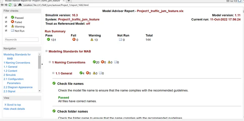
• Model Advisor Report is mandatory & this will be followed by Code Generation.
MODEL DEVELOPMENT ACCORDING TO REQUIREMENT
Signals and Calibration data:
Input Signals:
| Name of the Signal | Data Type | Range |
| Input_Voltage | uint8 | 0 - 255 |
| Input_Switch | boolean | 0 - 1 |
| Enable_Display | uint8 | 0 - 255 |
Output Signal:
| Name of the Signal | Data Type | Range |
| Output_Display | uint8 | 0 - 255 |
Calibration Signals:
| Name of the Signal | Data Type | Range | Initial Value |
| VOLTAGE_MINIMUM_RANGE | uint8 | 0 – 255 | 30 |
| VOLTAGE_MAXIMUM_RANGE | uint8 | 0 – 255 | 50 |
| OFF_MODE | uint8 | 0 – 255 | 2 |
| ON_MODE | uint8 | 0 – 255 | 1 |
| STANDBY_MODE | uint8 | 0 – 255 | 3 |
| INTERRUPT_1 | boolean | 0 – 1 | 1 |
| INTERRUPT_2 | boolean | 0 – 1 | 1 |
| NO_DISPLAY | uint8 | 0 – 255 | 0 |
Local Signal:
| Name of the Signal | Data Type | Range |
| Optimum_Voltage | boolean | 0 - 1 |
Requirement No 1:
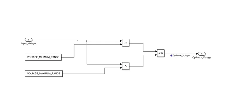
- Input Signal “Input_Voltage” is compared against voltage values “VOLTAGE_MINIMUM_RANGE” & “VOLTAGE_MAXIMUM_RANGE”.
- Incoming input signal “Input_Voltage” must be greater than – equal to “VOLTAGE_MINIMUM_RANGE” and less than – equal to “VOLTAGE_MAXIMUM_RANGE”.
- Output signal from here is “Optimum_Voltage” which will be one of the inputs to the subsystem “DisplayUnit”.
Requirement No 2 (DisplayUnit Subsystem):
- Input Signals are “Optimum_Voltage”, “Input_Switch”, and “Enable_Display”. Signal “Enable_Display” must be saturated between the range 0 – 7. The output signal from the subsystem is “Output_Display”.
- Input Signal “Enable_Display” is compared against a pre-defined set of values in a multiport switch. The total data ports in the multiport switch are 5.
- Multiport switch inputs 1 & 2 are connected to calibration signal “ON_MODE”, Multiport switch inputs 3 & 4 are connected to calibration signal “OFF_MODE” while Multiport switch input 5 is connected to calibration signal “STANDBY_MODE”.
- The output from the Multiport switch is connected to the first input port of the Switch block. The third input port of the Switch block is connected to the calibration signal “NO_DISPLAY”.
- Meanwhile NOT the value of the input signal “Input_Switch” is compared in an AND gate against the input signal “Optimum_Voltage” and the output from comparing if calibration signals “INTERRUPT_1” & “INTERRUPT_2” are equal. The output of the AND gate is the second input of the switch block.
- The output from the switch block is “Output_Display”.
MODEL DEVELOPMENT
Signals and Calibration data:
Input Signals:
| Name of the Signal | Data Type | Range |
| Input_Voltage | uint8 | 0 - 255 |
| Input_Switch | boolean | 0 - 1 |
| Enable_Display | uint8 | 0 - 255 |
Output Signal:
| Name of the Signal | Data Type | Range |
| Output_Display | uint8 | 0 - 255 |
Calibration Signals:
| Name of the Signal | Data Type | Range | Initial Value |
| VOLTAGE_MINIMUM_RANGE | uint8 | 0 – 255 | 30 |
| VOLTAGE_MAXIMUM_RANGE | uint8 | 0 – 255 | 50 |
| OFF_MODE | uint8 | 0 – 255 | 2 |
| ON_MODE | uint8 | 0 – 255 | 1 |
| STANDBY_MODE | uint8 | 0 – 255 | 3 |
| INTERRUPT_1 | boolean | 0 – 1 | 1 |
| INTERRUPT_2 | boolean | 0 – 1 | 1 |
| NO_DISPLAY | uint8 | 0 – 255 | 0 |
Local Signal:
| Name of the Signal | Data Type | Range |
| Optimum_Voltage | boolean | 0 - 1 |
Requirement No 1:
- Input Signal “Input_Voltage” is compared against voltage values “VOLTAGE_MINIMUM_RANGE” & “VOLTAGE_MAXIMUM_RANGE”.
- Incoming input signal “Input_Voltage” must be greater than – equal to “VOLTAGE_MINIMUM_RANGE” and less than – equal to “VOLTAGE_MAXIMUM_RANGE”.
- Output signal from here is “Optimum_Voltage” which will be one of the inputs to the subsystem “DisplayUnit”.
Requirement No 2 (DisplayUnit Subsystem):
- Input Signals are “Optimum_Voltage”, “Input_Switch”, and “Enable_Display”. Signal “Enable_Display” must be saturated between the range 0 – 7. The output signal from the subsystem is “Output_Display”.
- Input Signal “Enable_Display” is compared against a pre-defined set of values in a multiport switch. The total data ports in the multiport switch are 5.
- Multiport switch inputs 1 & 2 are connected to calibration signal “ON_MODE”, Multiport switch inputs 3 & 4 are connected to calibration signal “OFF_MODE” while Multiport switch input 5 is connected to calibration signal “STANDBY_MODE”.
- The output from the Multiport switch is connected to the first input port of the Switch block. The third input port of the Switch block is connected to the calibration signal “NO_DISPLAY”.
- Meanwhile NOT the value of the input signal “Input_Switch” is compared in an AND gate against the input signal “Optimum_Voltage” and the output from comparing if calibration signals “INTERRUPT_1” & “INTERRUPT_2” are equal. The output of the AND gate is the second input of the switch block.
- The output from the switch block is “Output_Display”.
MODEL DEVELOPMENT ACCORDING TO REQUIREMENT
Signals and Calibration data:
Input Signals:
| Name of the Signal | Data Type | Range |
| Input_Voltage | uint8 | 0 - 255 |
| Input_Switch | boolean | 0 - 1 |
| Enable_Display | uint8 | 0 - 255 |
Output Signal:
| Name of the Signal | Data Type | Range |
| Output_Display | uint8 | 0 - 255 |
Calibration Signals:
| Name of the Signal | Data Type | Range | Initial Value |
| VOLTAGE_MINIMUM_RANGE | uint8 | 0 – 255 | 30 |
| VOLTAGE_MAXIMUM_RANGE | uint8 | 0 – 255 | 50 |
| OFF_MODE | uint8 | 0 – 255 | 2 |
| ON_MODE | uint8 | 0 – 255 | 1 |
| STANDBY_MODE | uint8 | 0 – 255 | 3 |
| INTERRUPT_1 | boolean | 0 – 1 | 1 |
| INTERRUPT_2 | boolean | 0 – 1 | 1 |
| NO_DISPLAY | uint8 | 0 – 255 | 0 |
Local Signal:
| Name of the Signal | Data Type | Range |
| Optimum_Voltage | boolean | 0 - 1 |
Requirement No 1:
- Input Signal “Input_Voltage” is compared against voltage values “VOLTAGE_MINIMUM_RANGE” & “VOLTAGE_MAXIMUM_RANGE”.
- Incoming input signal “Input_Voltage” must be greater than – equal to “VOLTAGE_MINIMUM_RANGE” and less than – equal to “VOLTAGE_MAXIMUM_RANGE”.
- Output signal from here is “Optimum_Voltage” which will be one of the inputs to the subsystem “DisplayUnit”.
Requirement No 2 (DisplayUnit Subsystem):
- Input Signals are “Optimum_Voltage”, “Input_Switch”, and “Enable_Display”. Signal “Enable_Display” must be saturated between the range 0 – 7. The output signal from the subsystem is “Output_Display”.
- Input Signal “Enable_Display” is compared against a pre-defined set of values in a multiport switch. The total data ports in the multiport switch are 5.
- Multiport switch inputs 1 & 2 are connected to calibration signal “ON_MODE”, Multiport switch inputs 3 & 4 are connected to calibration signal “OFF_MODE” while Multiport switch input 5 is connected to calibration signal “STANDBY_MODE”.
- The output from the Multiport switch is connected to the first input port of the Switch block. The third input port of the Switch block is connected to the calibration signal “NO_DISPLAY”.
- Meanwhile NOT the value of the input signal “Input_Switch” is compared in an AND gate against the input signal “Optimum_Voltage” and the output from comparing if calibration signals “INTERRUPT_1” & “INTERRUPT_2” are equal. The output of the AND gate is the second input of the switch block.
- The output from the switch block is “Output_Display”.
Designing MATLAB Simulink Model:
requrement_1
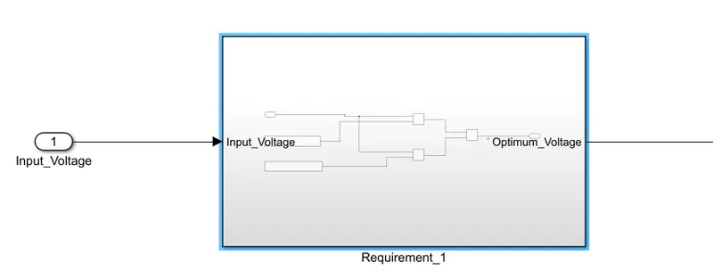
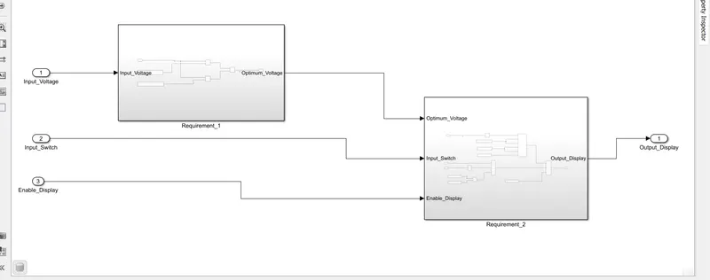
- Input Signal “Input_Voltage” is compared against voltage values “VOLTAGE_MINIMUM_RANGE” & “VOLTAGE_MAXIMUM_RANGE”. Then their outputs are given as the input for AND block, the Output of which is Optimum_Voltage.
Requirement2:
- Optimum_Voltage from the Req1, “Input_Switch”, and “Enable_Display” are the Input Signals. The output signal from the subsystem is “Output_Display”.
- Signal “Enable_Display” must be saturated between the range 0 – 7.
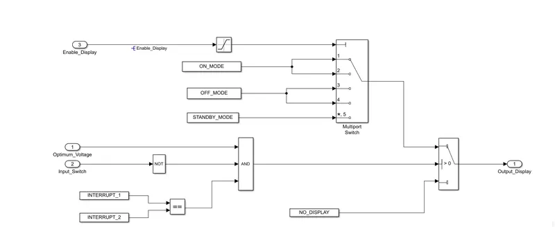
- Input Signal “Enable_Display” is compared against a pre-defined set of values in a multiport switch. The total data ports in the multiport switch are 5. Multiport switch inputs 1 & 2 are connected to calibration signal “ON_MODE”, Multiport switch inputs 3 & 4 are connected to calibration signal “OFF_MODE” while Multiport switch input 5 is connected to calibration signal “STANDBY_MODE”. The output from the Multiport switch is connected to the first input port of the Switch block. The third input port of the Switch block is connected to the calibration signal “NO_DISPLAY”.
- Meanwhile NOT the value of the input signal “Input_Switch” is compared in an AND gate against the input signal “Optimum_Voltage” and the output from comparing if calibration signals “INTERRUPT_1” & “INTERRUPT_2” are equal. The output of the AND gate is the second input of the switch block.
- The output from the switch block is “Output_Display”.
FINAL MODEL OF TRAFFIC JAM ASSISTANT FEATURE
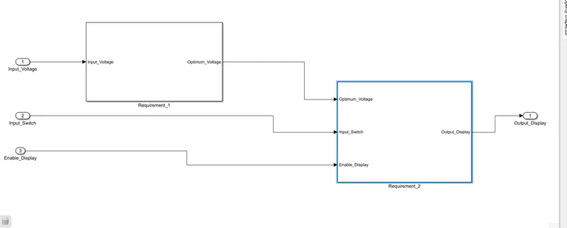
FOR SAFETY PURPOSE WE HIDE THE SUBSYSTEM BY USING MASKED
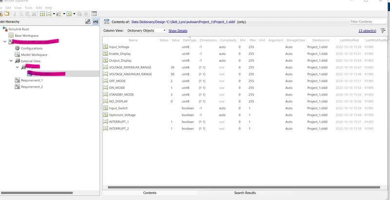
NOW CREATE THE SLDD FOR MODEL
- Goes to modeling tab and open
- select the link to ndata dictionary
- then create new
- choose design data and assign data according given input and output of data
- then load inside the model , if alredy load the SLDD then not required.
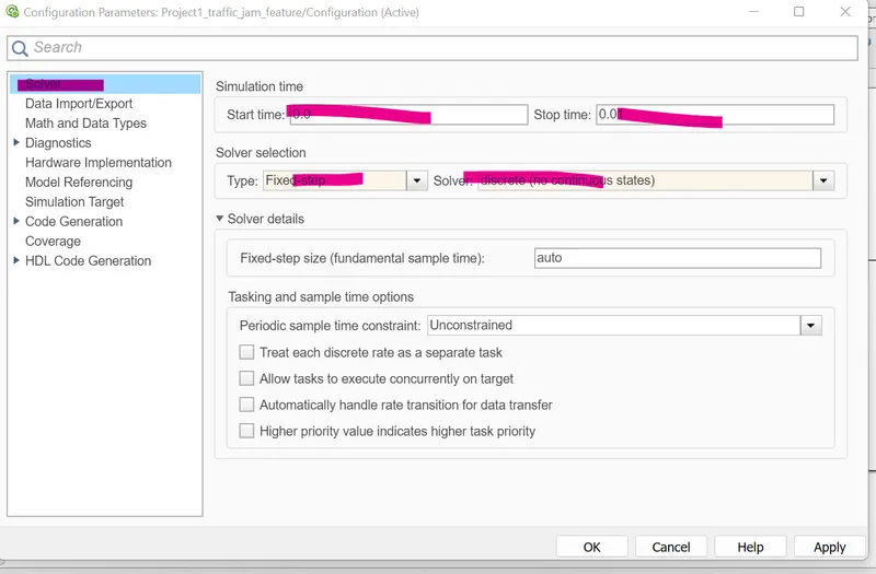
Solver seting of model
code generation seting
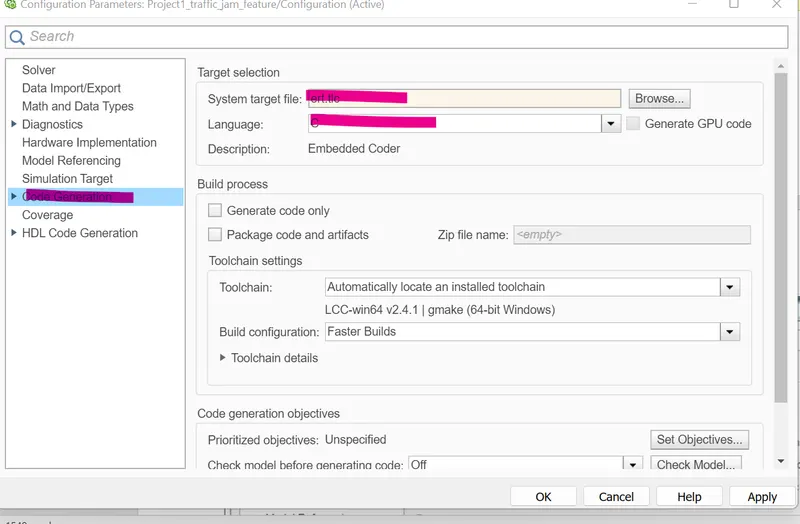
FOR C-CODE GENERATE FOLLOWING ARE STEPS
- Click on "APP" tab
- select embeded coder
- then click on "BUILD"
- And wait until code not generate
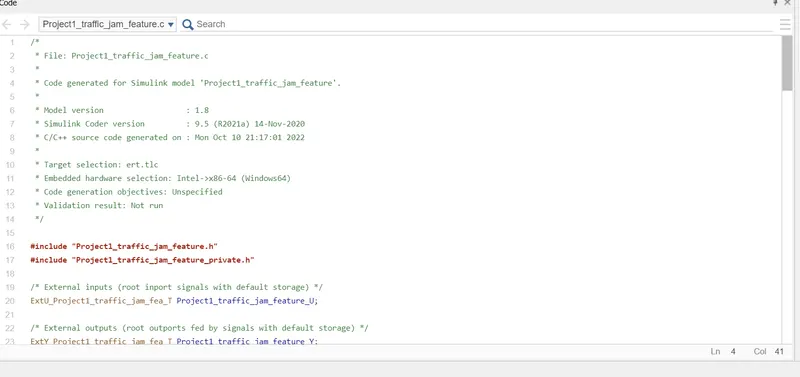
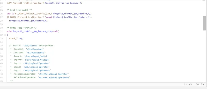
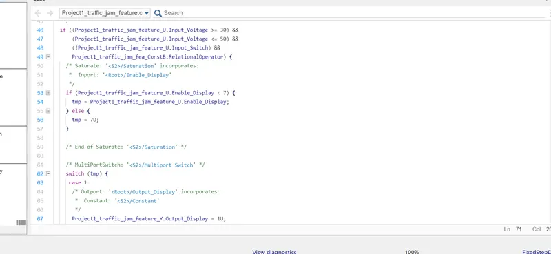
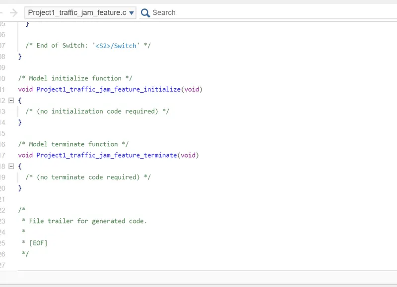
This model developed in MATLAB Simulink as per MBD guidelines and advoisory report
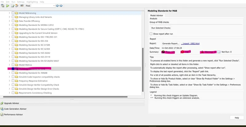
Following are Model Advisor Report
steps
- modeling
- model advisor
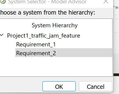
- select "by task"
- select one option "mab guidelines"
- then run model and wait for result