Project 1
- Choosing any three topologies from the above given and developing them in the simulink :-
1) Buck CCM :-
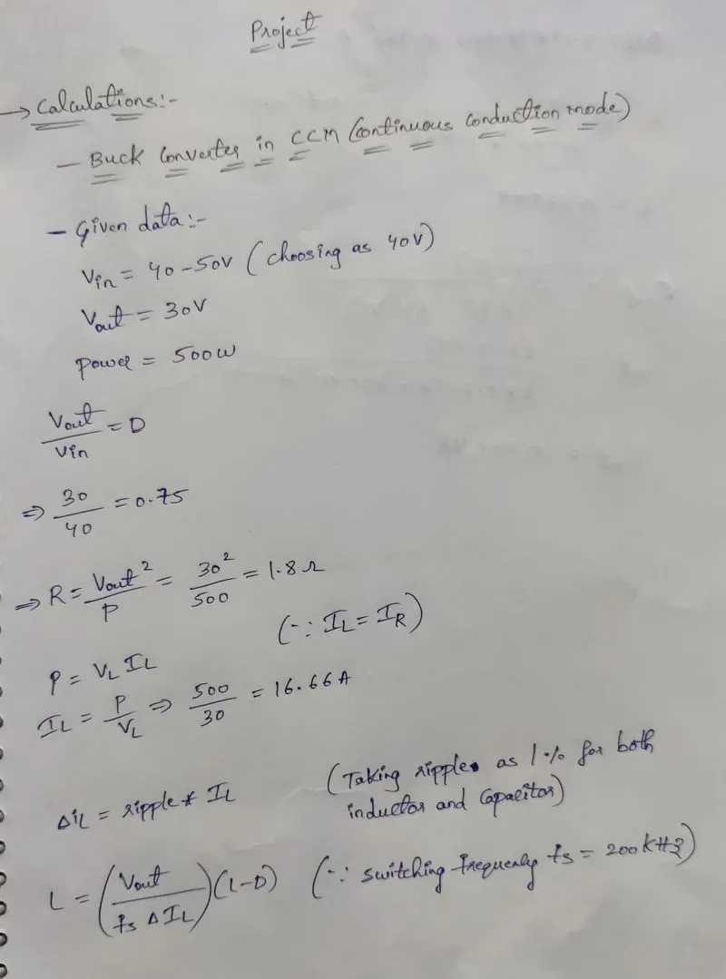
Given data :-
Input voltage = 40-50 V
Output voltage = 30 V
Power =500 W
- The schematic diagram for the above converter is shown below :-
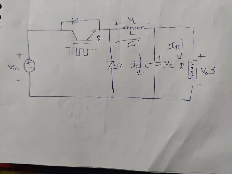
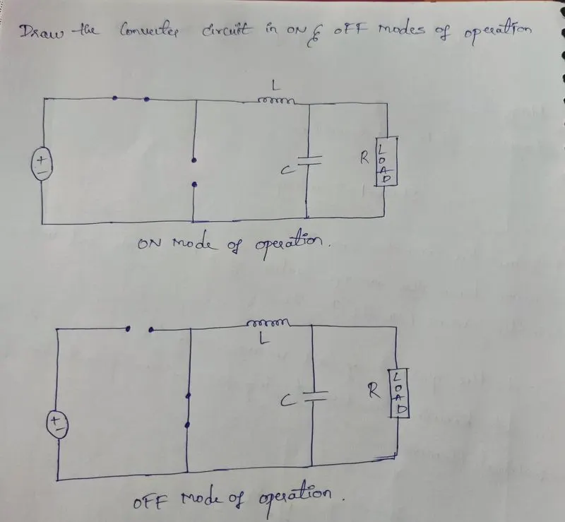
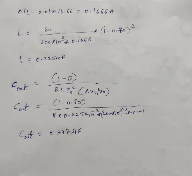
- To design the above buck converter we need to design inductor, capacitor and resistor and the calculations required to find them are shown below :-
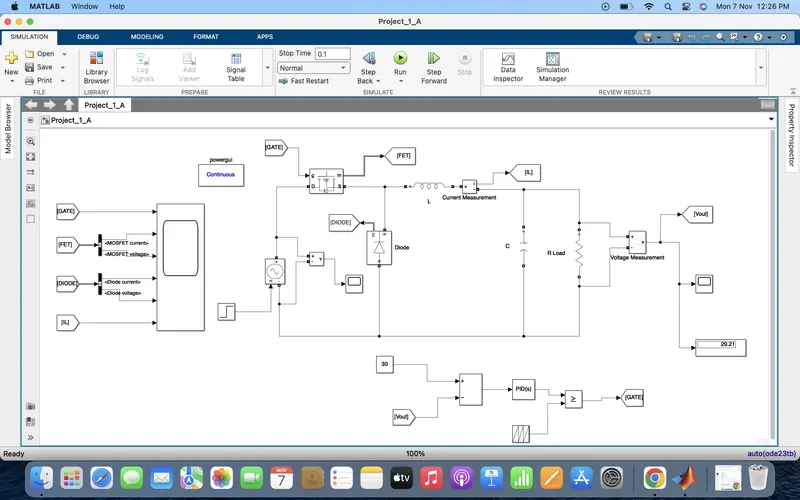
-Now the simulink model build is shown with the above parameters :-
-All the designed parameters set to the block are shown below :-
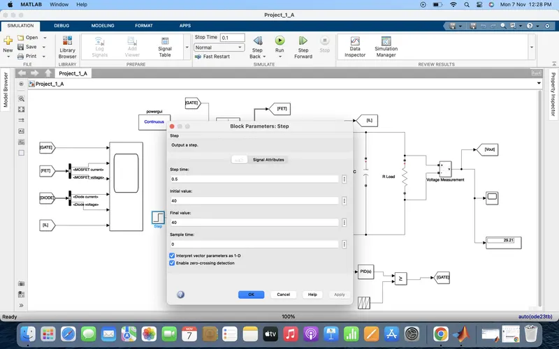
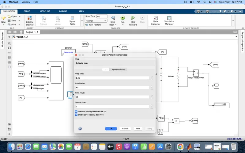
1) Step block :-
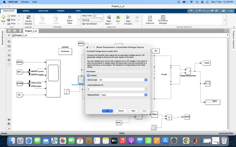
2) Controlled voltage source :-
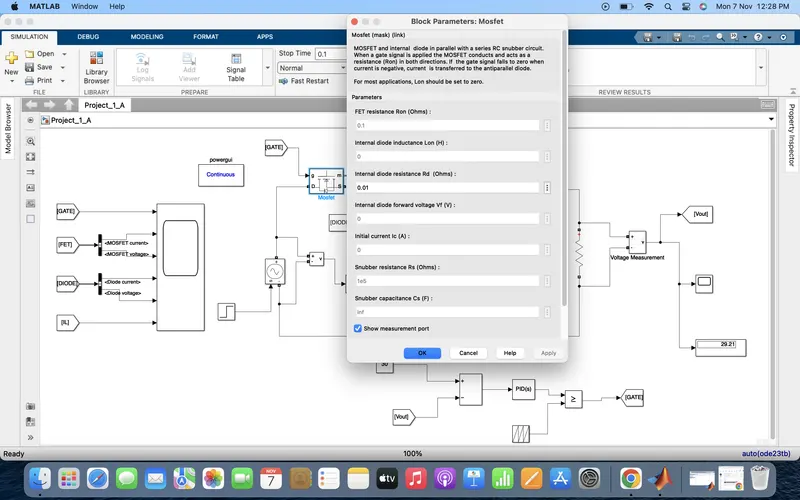
3) MOSFET :-
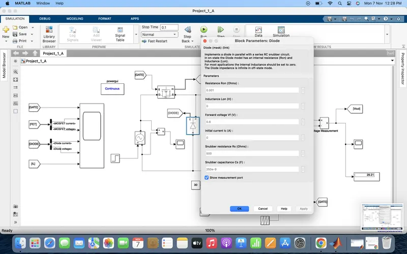
4) DIODE :-
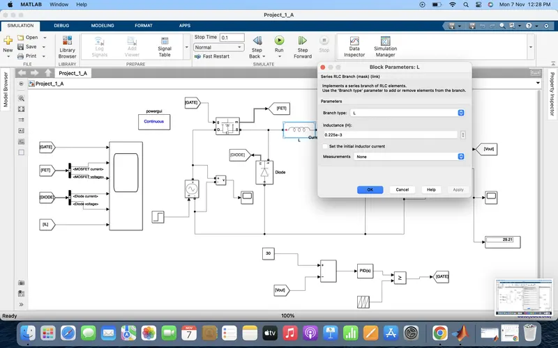
5) Inductor :-
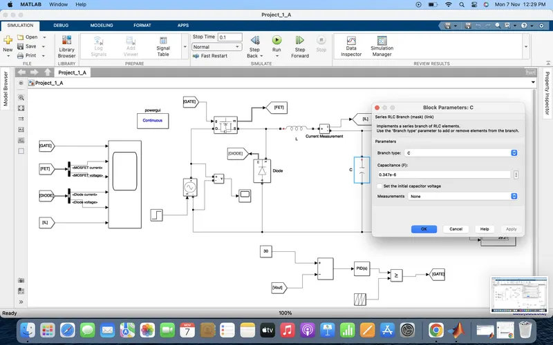
6) Capacitor :-
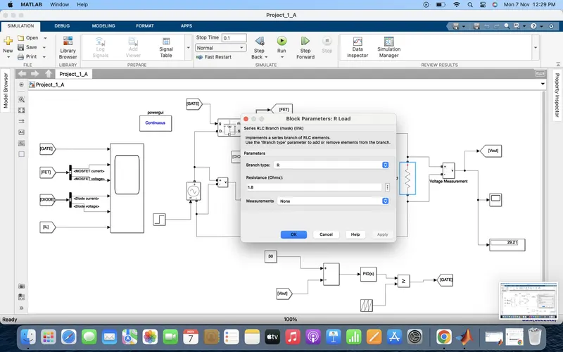
7) Resistor (Load):-
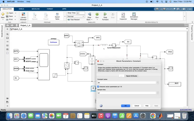
8) Constant :-
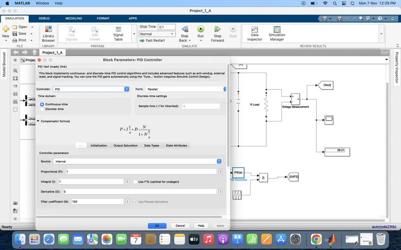
9) PID controller :-
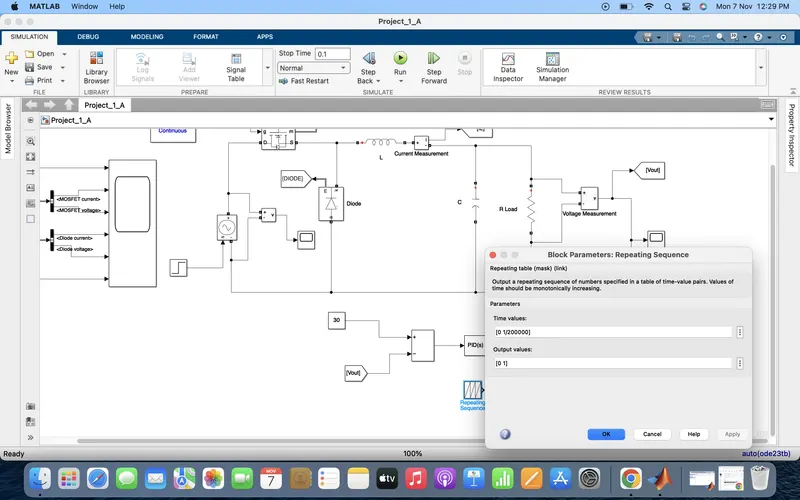
10) Repeating sequence :-
-With the above designed parameters the simulink model is run with a stop time of 0.1 second.
Here in order to check the dynamic conditions of the converter, we are desigining the feedback also and we will check them by two cases as follows :-
case-1 :- Vin = 40 V, Vout = 30 V
- The results are shown in the below graphs :-
- Input voltage :- 40 V
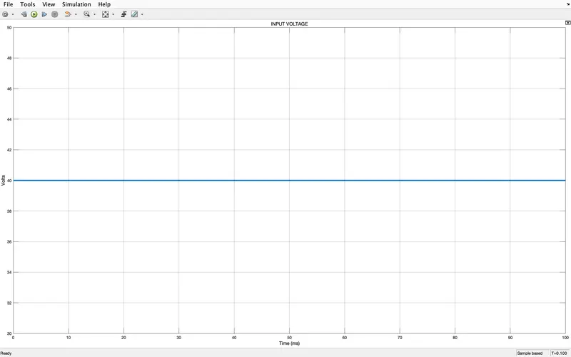
- Output voltage :- 30V
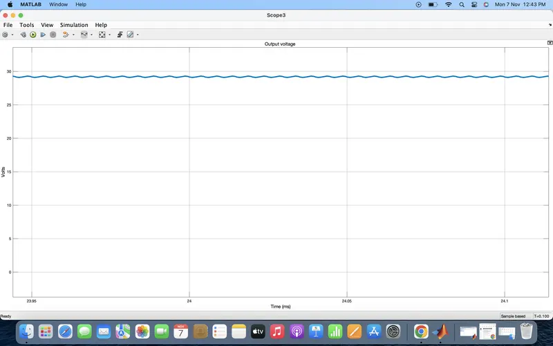
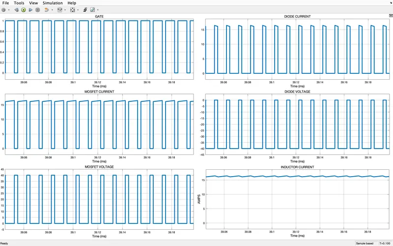
- MOSFET, DIODE, GATE, and INDUCTOR current and voltages :-
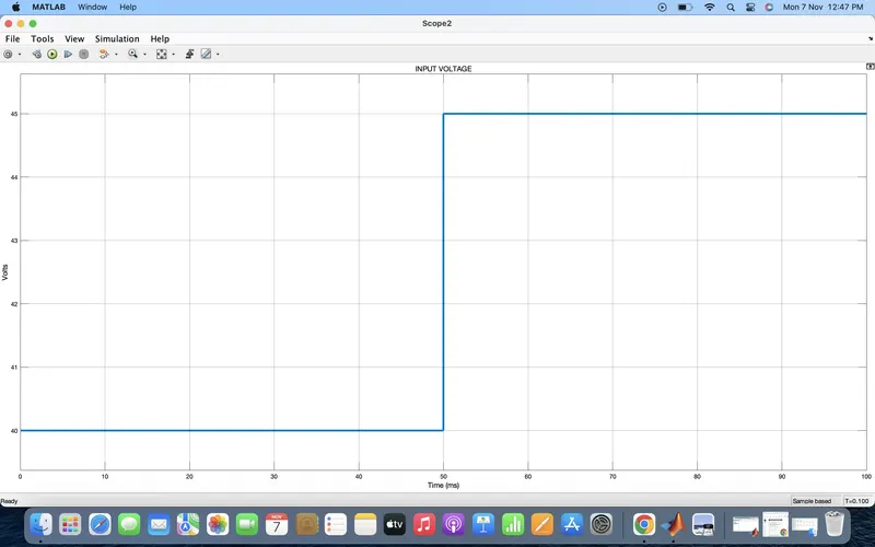
-Case-2 :- Now we are changing the input to 45 V at time 0.05 seconds and checking the output.
-Input voltage :-
- Output voltage :-
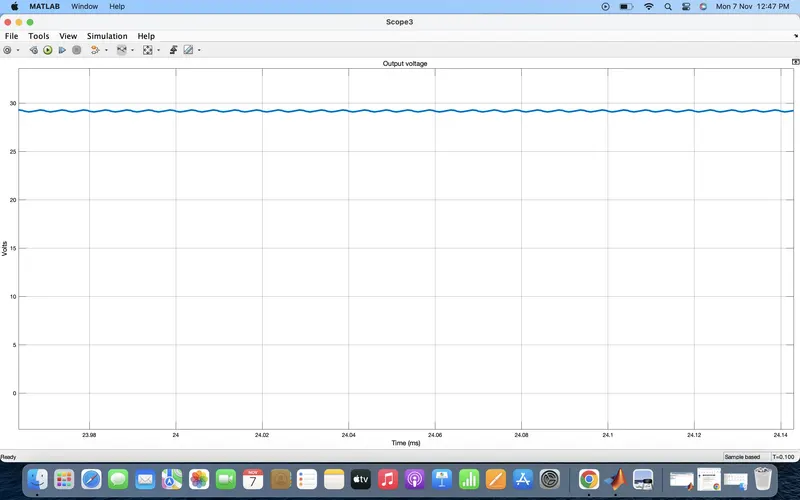
we can see from the below graph that even if we change the input to 45V at t = 0.05 seconds we are getting almost the same output of 30 V as before.
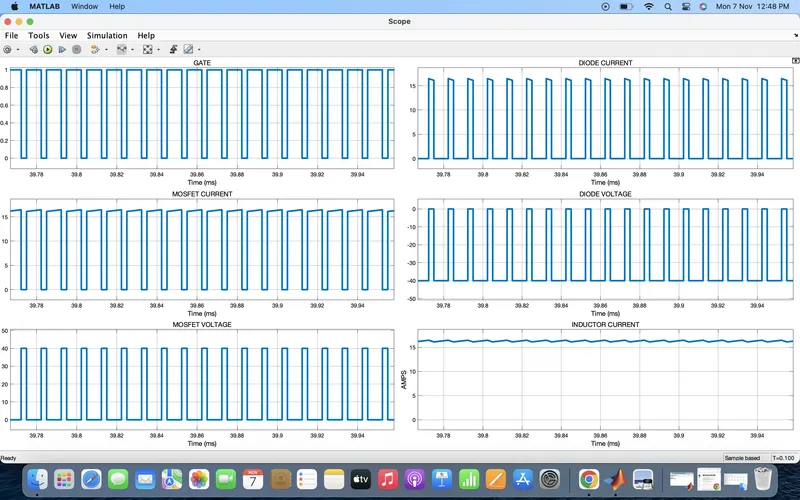
- MOSFET, DIODE, Inductor, GATE, voltages and currents are shown below :-
2) Boost CCM :-
Given data :-
Input voltage :- 20-30 V
Output voltage :- 40 V
Power :- 600 W
- The schematic diagram of boost converter is shown below :-
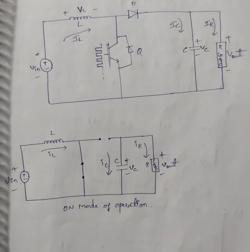
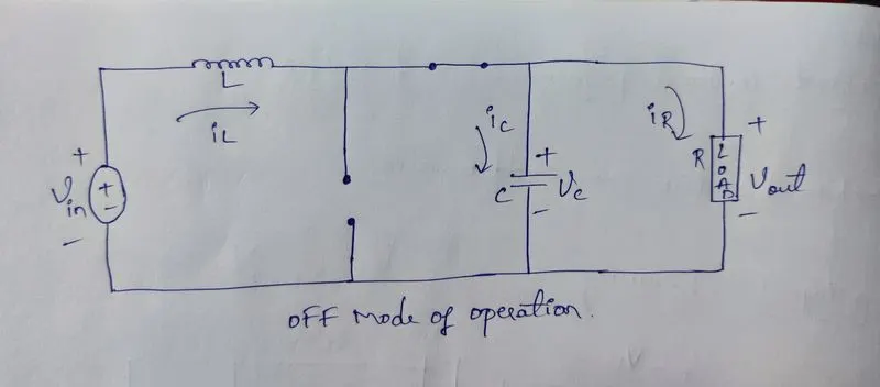
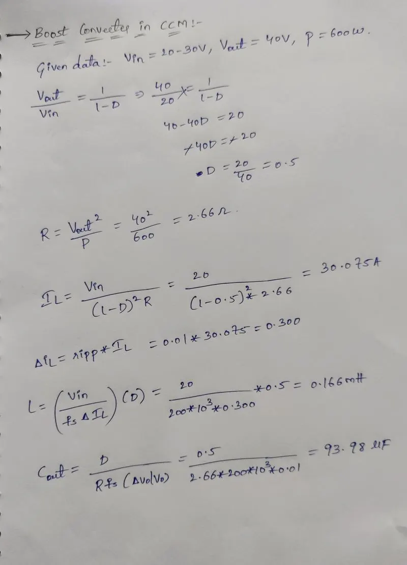
-The required calculations to design the boost converter are shown below :-
- With the above calculated parameters an simulink model is designed and is shown below :-
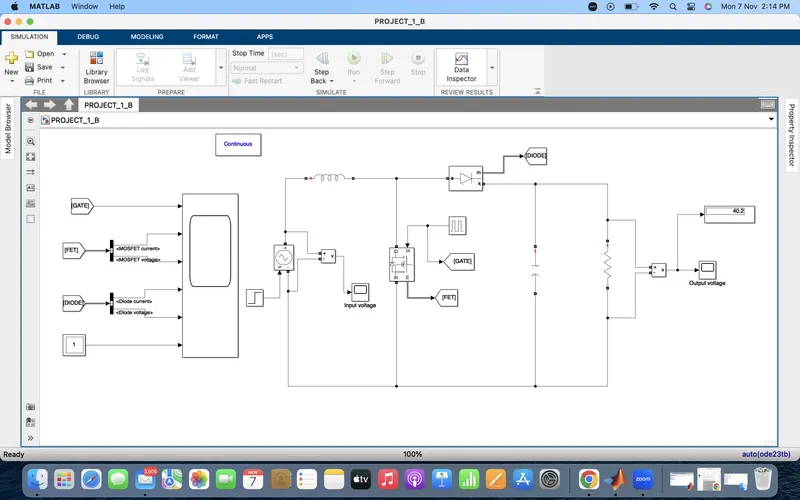
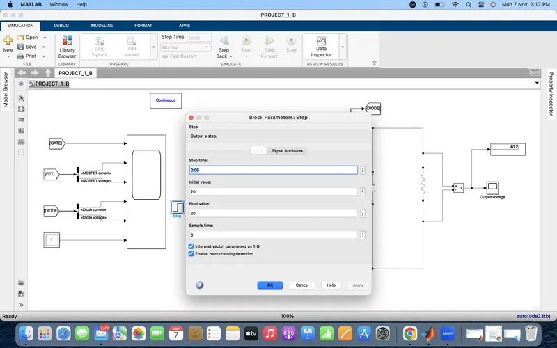
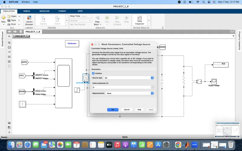
- All the designed parameter blocks are shown below :-
1) Step :-
2) Controlled voltage source :-
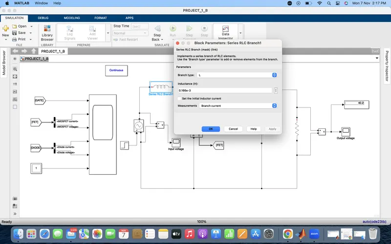
3) Inductor :-
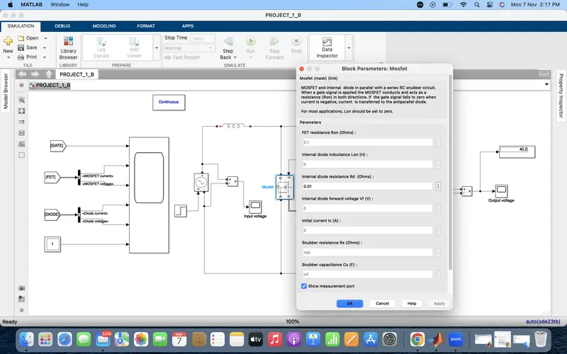
4) MOSFET :-
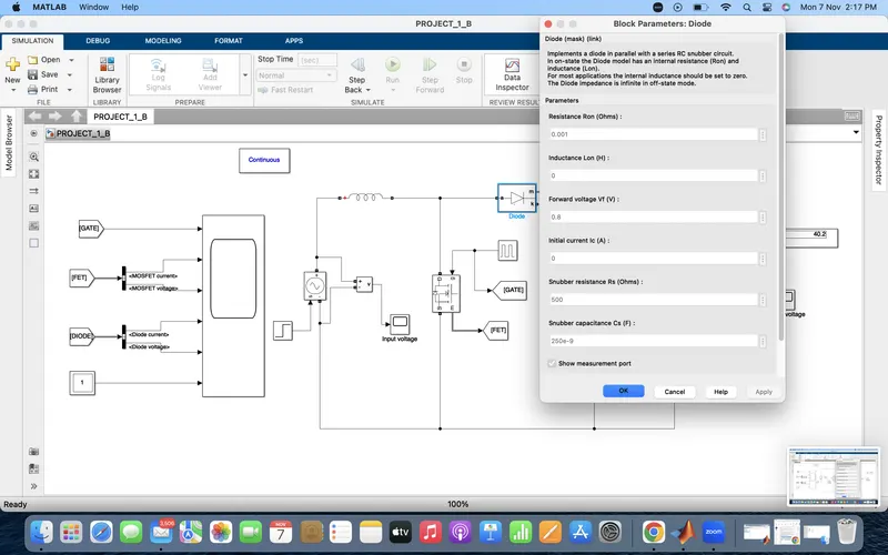
5) DIODE :-
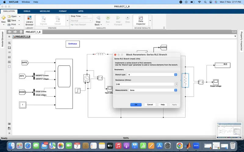
6) Resistor :-
7) Capacitor :-
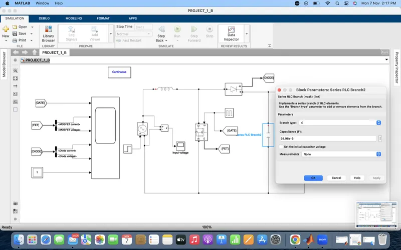
8) Pulse generator :-
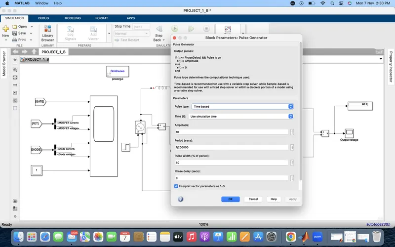
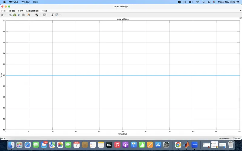
- With the above parameters the simulink model is designed and run with stop time of 0.1 second and results are shown below :-
- Input voltage :- 20 V
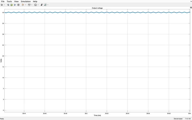
- Output voltage :-
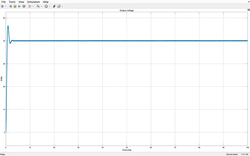
- We can see that we are getting the output of 40 V.
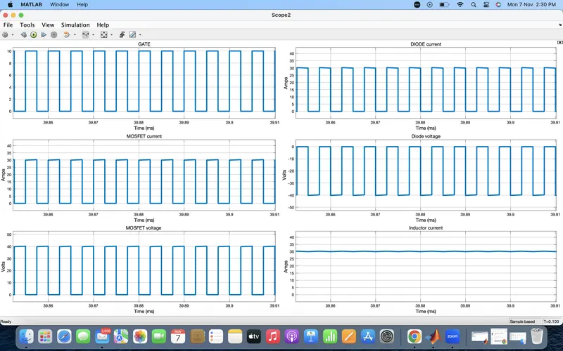
- Gate, MOSFET, DIODE, Inductor currents and voltages are shown below :-
10) Buck CCM :-
Given data :-
Input voltage :- 400-500 V
Output voltage :- 300 V
Power :- 5 KW
- The schematic diagram for buck converter is shown below :-
- The required calculations to design inductor, capacitor and resistor are shown below :-
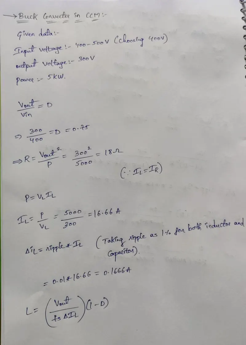
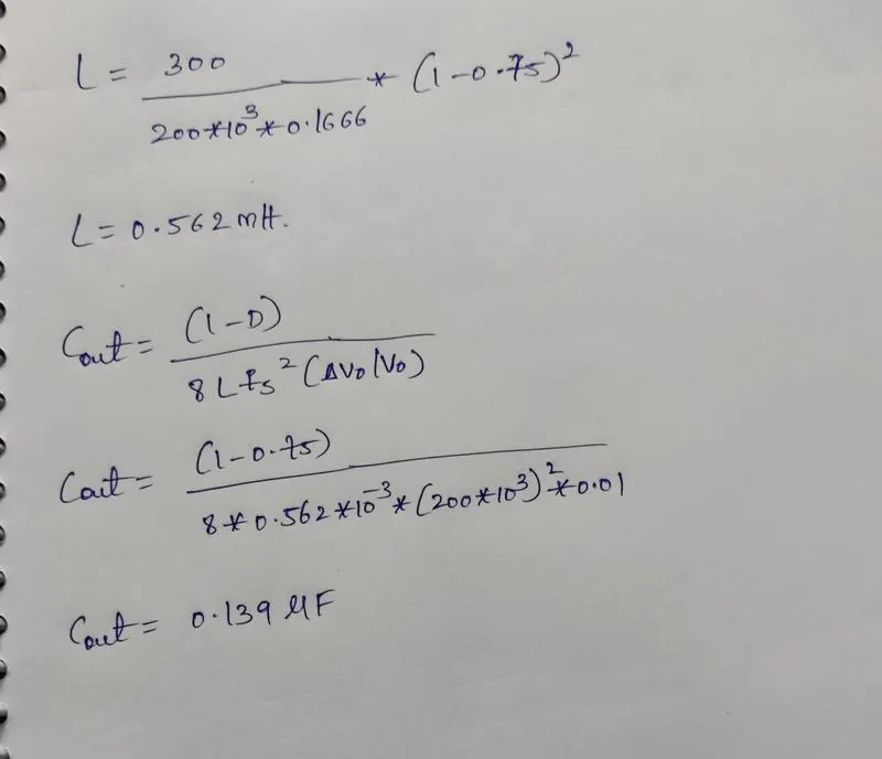
- With the above calculated values the simulink model is designed and is shown below :-
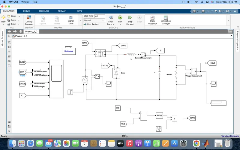
- All the block parameters are shown below :-
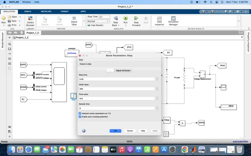
1) Step :-
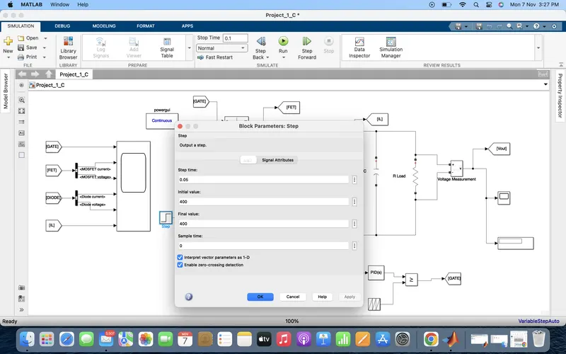
2) Controlled voltage source :-
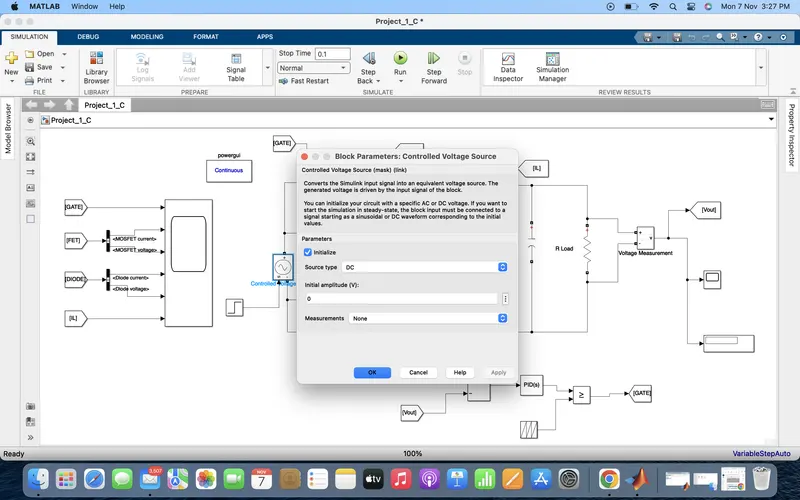
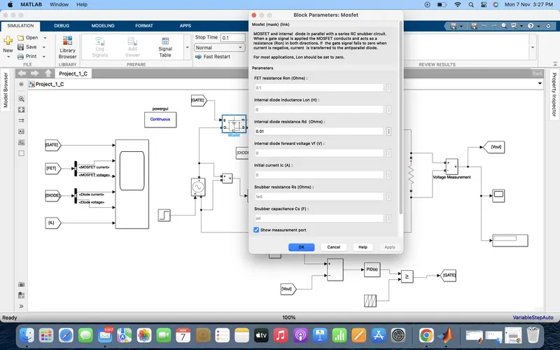
3) MOSFET :-
4) Capacitor :-
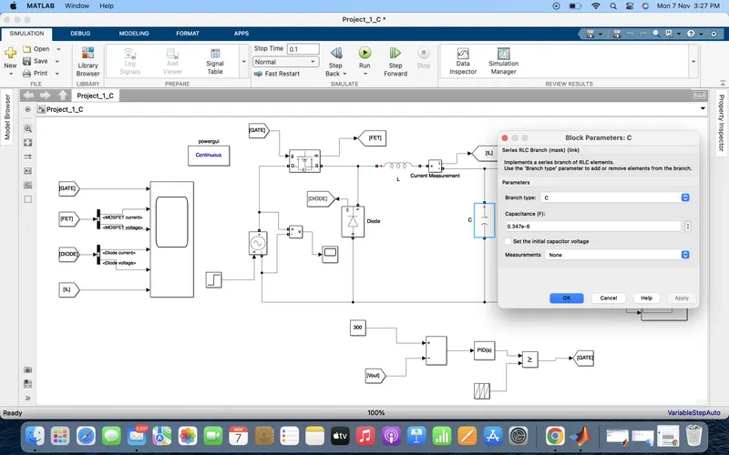
5) Resistor :-
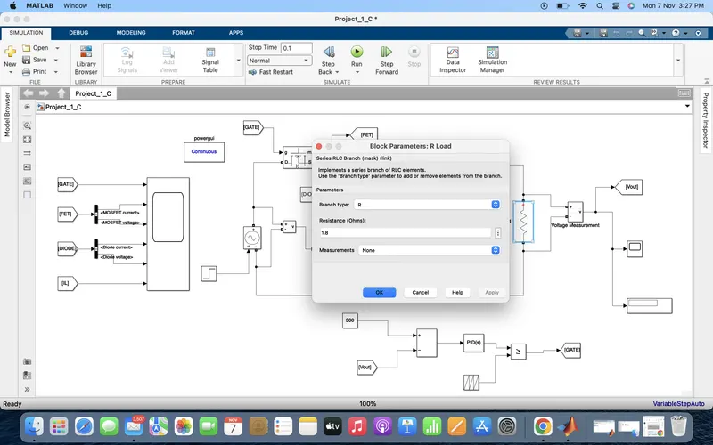
6) Inductor :-
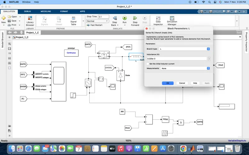
7) Constant :-
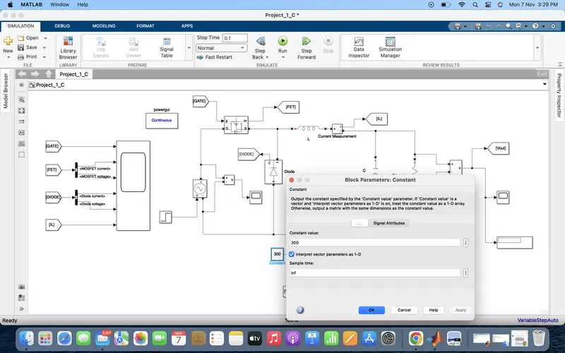
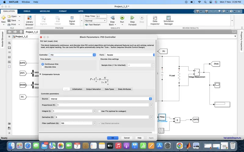
8) PID :-
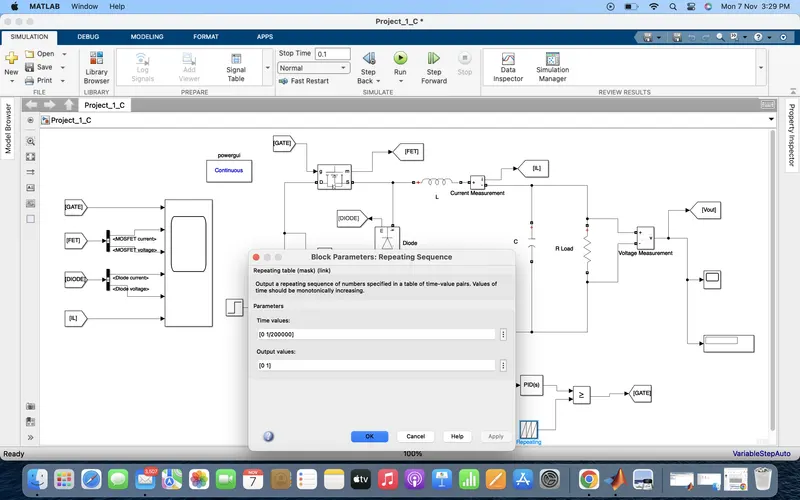
9) Repeating sequence :-
- The above designed model is run with stop time of 0.1 second and results are shown below :-
- In order to get the stability in dynamic conditions we have designed feedback system and that results is obtained by two cases as follows :-
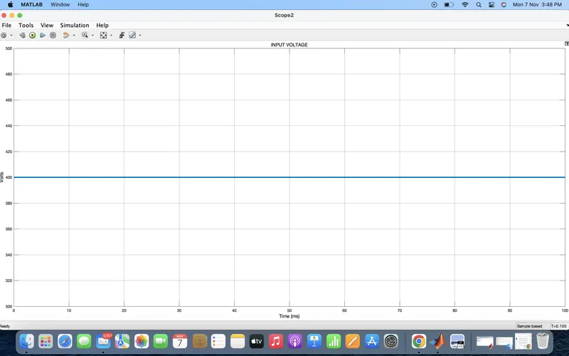
- Case-1 :- Vin = 400 V , Vout = 300 V, Power = 5000 W
- The results are shown below :-
- Input voltage :-
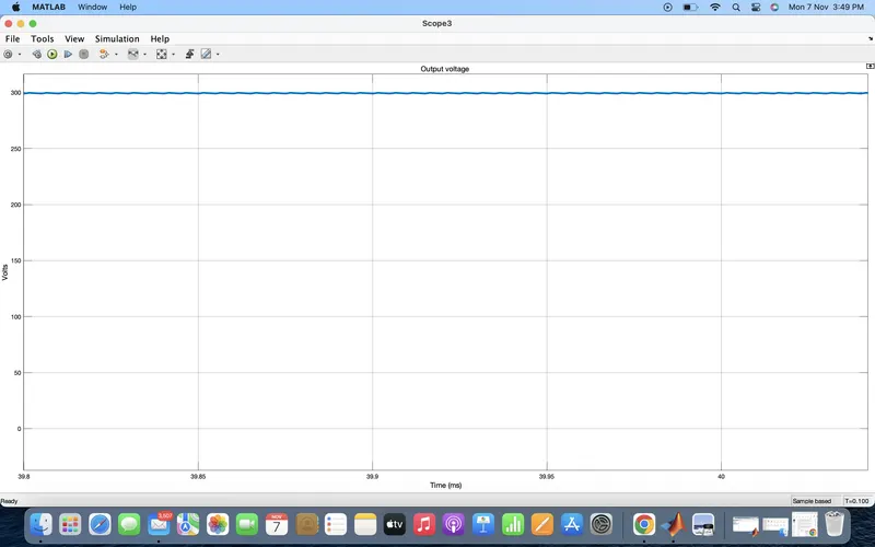
- Output voltage :-
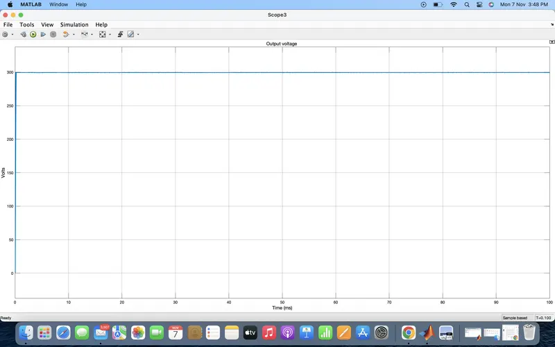
- We can see that we got the output voltage of 300 V.
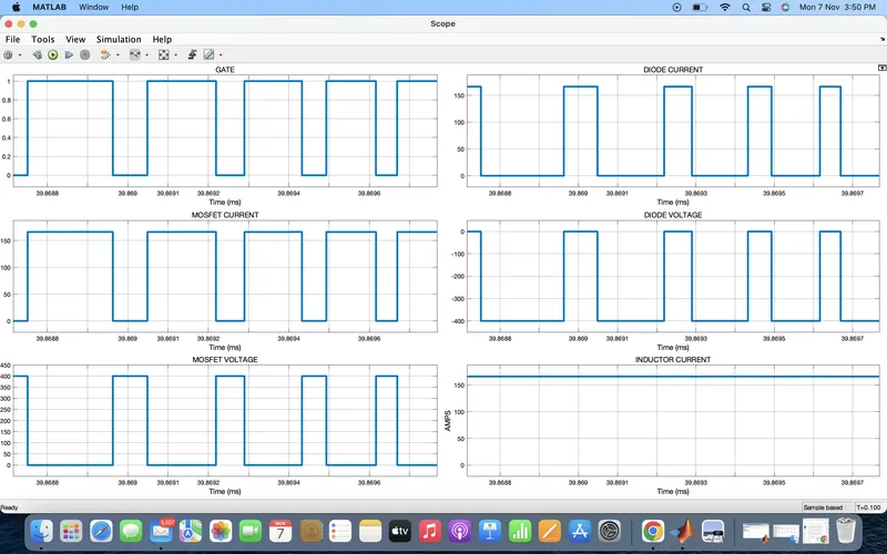
- GATE, MOSFET, DIODE, Inductor current and voltages :-
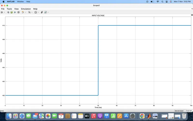
- Now we are changing the input to 410 V at time t = 0.05 seconds and checking the output.
- Input voltage
- Output voltage :-
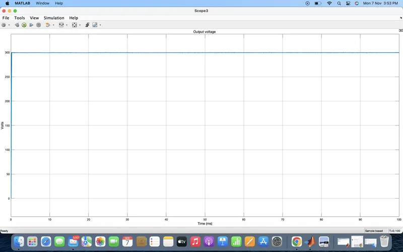
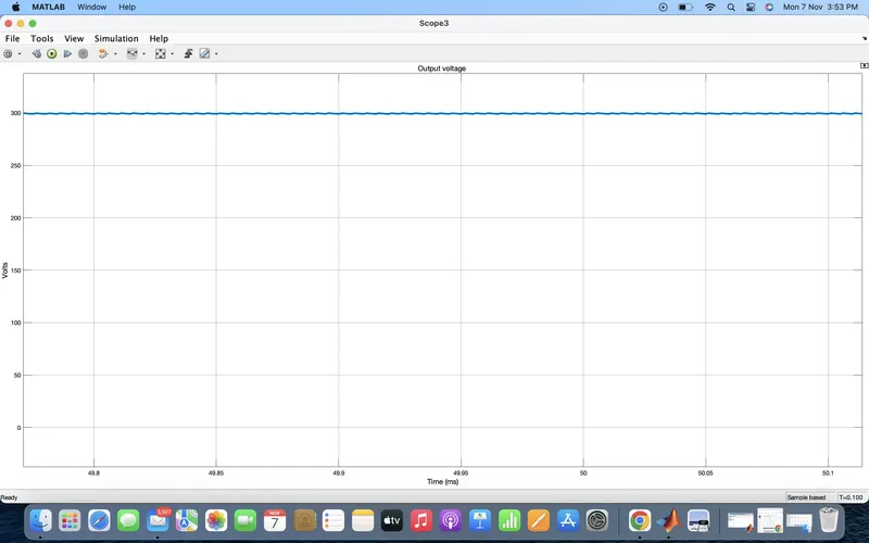
- We an see that even after changing the input to 410 V we got the output of 300 V.
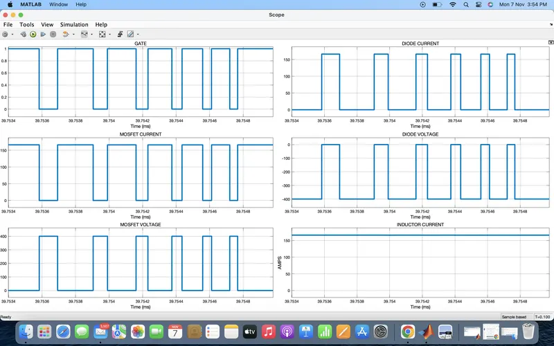
- GATE, MOSFET, DIODE, Inductor currents and voltages :-
- Hence we have designed 3 topologies from the above given topologies and simulated them in the simulink and shown the neccessary waveforms successfully.