Project 1
1) Sol:- To design the Buck converter in Continuous Conduction Mode(CCM) using MATLAB(Simulink)
The design reqiurements are as follows:
- Vi= 40-50 V
- Vout= 30 V
- Po= 500 watts
- fs=50 kHz
- `deli_L le 25% of I_L`
- `delv_c le 5%` of `V_o`
For Buck converter we have , output voltage= Vo=D*Vi -----(1)
Load resistance=R=`V_o^2/P_o=30^2/500=1.8`
R=1.8 ohms ------(2)
Output Current=Io=`P_o/V_o=500/30=16.67`
Io=16.67 A --------(3)
But under steadystate condition the inductor average current =`I_L=I_o`
using the equation (3) , `I_L=16.67 A` -------(4)
Now the Ripple inductor current is given by , `delI_L= 25 %`of `I_L`
Using equation(4) , `delI_L= 25/(100)(16.67)`
`delI_L=4.167 A` ----------(5)
Capacitor voltage ripple is given by
`delV_c= 5 % of Vo`
`delV_c=5/100(30) = 1.5 V`------------(6)
Determine Duty ratio:
As the input voltage is varying , so does the duty ratio as to vary to maintain the output voltage constant accordingly.
Dmax:
When Vi=40 V ,
using equation(1) `D_max=V_0/V_i=30/40=0.75`
Dmax=0.75 ----------(7)
Dmin:
When Vi=50 V ,
using equation(1) `D_min=V_0/V_i=30/50=0.6`
Dmin=0.6 ----------(8)
Inductor design(L):
To maintain the circuit to operate in continuous conduction mode(CCM) , the critical inductance required is given as,
`L_(cr)=V_o/(f_s*delI_L)(1-D)` ----------(9)
- For Vi=40 V and Dmax=0.75 :
`L_(cr)=30/(50e3*4.167)(1-0.75)`
`L_(cr)=36e-6 H` -----------------------(10)
- For Vi=50 V and Dmin=0.6 :
`L_(cr)=30/(50e3*4.167)(1-0.6)`
`L_(cr)=57.6e-6 H` -----------------------(11)
Hence , for worst case scenario i.e., to have the continuous current through inductor . The value of inductance is :
L> max{ equation(9), equation(10) }
L> max{ 36 microH, 57.6 microH }
Therefore , let the value of L= 100 microH -------------(12)
Capacitor Design(C):
The critical capacitance required to maitain the output voltage ripple low as the design requirement.
`C_(cr)=(1-D)V_o/(8L_(cr)f_s^2delV_c)`
- For Vi=40 V and Dmax=0.75 :
`C_(cr)=(1-0.75)*30/(8(100e-6)(50e3)^2(1.5))`
`C_(cr)=2.5e-6 F`-----------------------(13)
- For Vi=50 V and Dmin=0.6 :
`C_(cr)=(1-0.6)*30/(8(100e-6)(50e3)^2(1.5))`
`C_(cr)=4e-6 F`-----------------------(13)
Hence, for maitaining the voltage ripple less than 5% , we need to have a capacitance which is greater the both cases values.
Therefore, C> Max{ equation(12), equation(13) }
C> Max{2.5 microF , 4 microF }
Let, the value of capacitance is C= 10 microF.
Specifications of Buck converter:
- L=100e-6 H
- C=10e-6 F
- R=1.8 ohms
- fs=50 kHz
- Vi=40 - 50 V
- P=500 watts
Simulink model of Buck converter:
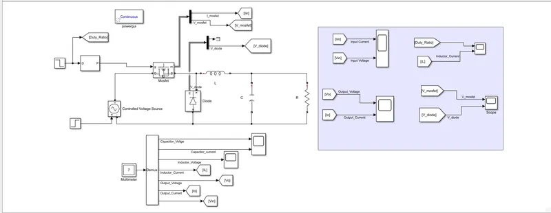
Fig-01: The simulink model for Buck Converter
As the input voltage is varying the step function is used to vary the input from 40 V to 50 V at t=0.0025 sec , same with the duty ratio D= 0.75 to 0.6 at t=0.0025 sec and generating accordingly the pulses to turn ON and OFF the MOSFET and thus to maintain the output voltage constant at Vo=30 V.
Results:
1.Output voltage and current waveforms:
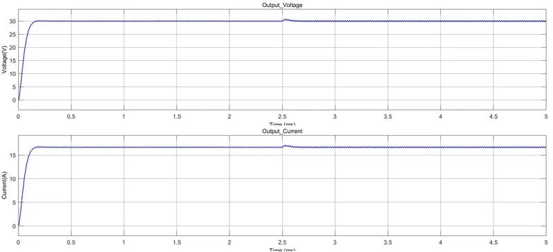
Fig-02: Waveforms of Output voltage and current for Buck converter.
From the above waveforms we can observe the output voltage almost 30 V , due to the internal resistance of the switching devices the output voltage is not exactly 30 V. And at t=0.0025 sec we can observe small overshoot during transient and settles down in the steadystate.
2.Input Voltage and Current waveforms:
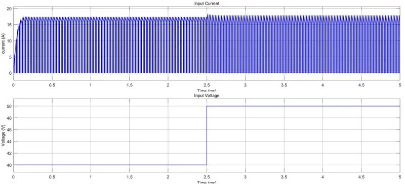
Fig-03: Waveforms of Input voltage and current for Buck converter.
At t=2.5 msec , the input voltage is varied from 40 to 50 V. Here, the input current is pulsating DC waveform. Hence, to make input a pure DC value we need to add the input filter.
3. Inductor current and Duty ratio waveform:
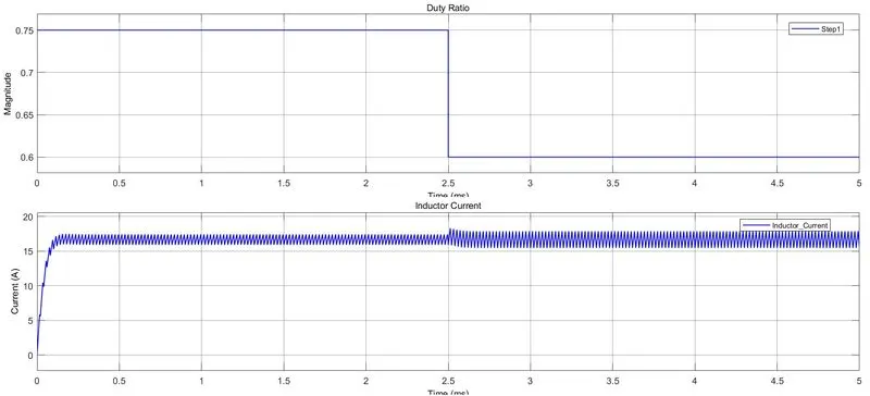
Fig-04: Waveforms of Inductor current and Duty ratio for Buck converter.
According to design requirement the inductor current ripple is maitained below 25% of Average inductor current and it is in Continuous conduction mode(CCM).
4. MOSFET and Diode Voltage waveform:
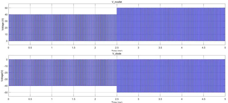
Fig-05: Waveforms of MOSFET and Diode Voltage for Buck converter.
From the above waveforms we can observe that the maximum breakdown voltage of devices. Hence, we can choose the breakdown voltage ratings of swiching devices accordingly.
2) Sol:- To design the Boost converter in Continuous Conduction Mode(CCM) using MATLAB(Simulink)
The design reqiurements are as follows:
- Vi= 20-30 V
- Vout= 40 V
- Po= 600 watts
- fs=50 kHz
- `deli_L le 25% of I_L`
- `delv_c le 5%` of `V_o`
For Boost converter we have , output voltage= Vo=`(V_i)/(1-D)` -----(1)
Load resistance=R=`V_o^2/P_o=40^2/600=2.667`
R=2.667 ohms ------(2)
Output Current=Io=`P_o/V_o=600/40=15`
Io=15 A --------(3)
Determine Duty ratio:
As the input voltage is varying , so does the duty ratio as to vary to maintain the output voltage constant accordingly.
Dmax:
When Vi=20 V ,
using equation(1) `D_max=1-V_i/V_o=1-20/40=0.5`
Dmax=0.5 ----------(4)
Dmin:
When Vi=30 V ,
using equation(1) `D_min=1-V_i/V_o=1-30/40=0.25`
Dmin=0.25 ----------(5)
But under steadystate condition the inductor average current =`I_L=(I_o)/(1-D)` ----(6)
Inductor average current(`I_L`):
For Dmax=0.5:
Using equations (3),(4)&(6)
`I_L=(I_o)/(1-D_max)=15/(1-0.5)=30`
`I_L=30 A`---------------(7)
For Dmax=0.5:
Using equations (3),(5)&(6)
`I_L=(I_o)/(1-D_min)=15/(1-0.25)=20`
`I_L=20 A`---------------(8)
Now the Ripple inductor current is given by , `delI_L= 25 %`of `I_L` ----------(9)
For Dmax=0.5:
Using equations (7)&(9)
`delI_L= 25/(100)(30)`
`delI_L=7.5 A` ----------(10)
For Dmax=0.25:
Using equations (8)&(9)
`delI_L= 25/(100)(20)`
`delI_L=5 A` ----------(11)
Capacitor voltage ripple is given by
`delV_c= 5 % of Vo`
`delV_c=5/100(40) = 2 V`------------(12)
Inductor design(L):
To maintain the circuit to operate in continuous conduction mode(CCM) , the critical inductance required is given as,
`L_(cr)=(V_i/(f_s*delI_L))(D)` ----------(13)
- For Vi=20 V ,Dmax=0.5 and `delI_L=7.5 A` :
`L_(cr)=(20/(50e3*7.5))(0.5)`
`L_(cr)=26.66e-6 H` -----------------------(14)
- For Vi=30 V , Dmin=0.25 and `delI_L=5 A`:
`L_(cr)=(30/(50e3*5))(0.25)`
`L_(cr)=30e-6 H` -----------------------(15)
Hence , for worst case scenario i.e., to have the continuous current through inductor . The value of inductance is :
L> max{ equation(14), equation(15) }
L> max{ 26.67 microH, 30 microH }
Therefore , let the value of L= 59 microH -------------(16)
Capacitor Design(C):
The critical capacitance required to maitain the output voltage ripple low as the design requirement.
`C_(cr)=(D)V_o/(R*f_s(delV_c))`
- For Vi=20 V and Dmax=0.5 :
`C_(cr)=(0.5)*40/((2.67)(50e3)(0.05))`
`C_(cr)=75e-6 F`-----------------------(17)
- For Vi=30 V and Dmin=0.25 :
`C_(cr)=(0.25)*40/((2.67)(50e3)(0.05))`
`C_(cr)=37.5e-6 F`-----------------------(18)
Hence, for maitaining the voltage ripple less than 5% , we need to have a capacitance which is greater the both cases values.
Therefore, C> Max{ equation(17), equation(18) }
C> Max{75 microF , 37.5 microF }
Let, the value of capacitance is C= 100 microF.
Specifications of Boost converter:
- L=50e-6 H
- C=100e-6 F
- R=2.67 ohms
- fs=50 kHz
- Vi=20 - 30 V
- P=600 watts
Simulink model of Boost converter:
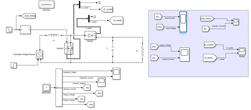
Fig-01: The simulink model for Boost Converter
As the input voltage is varying the step function is used to vary the input from 20 - 30 V at t=5 msec , same with the duty ratio D= 0.5 to 0.25 at t=5 msec and generating accordingly the pulses to turn ON and OFF the MOSFET and thus to maintain the output voltage constant at Vo=40 V.
Results:
1.Output voltage and current waveforms:
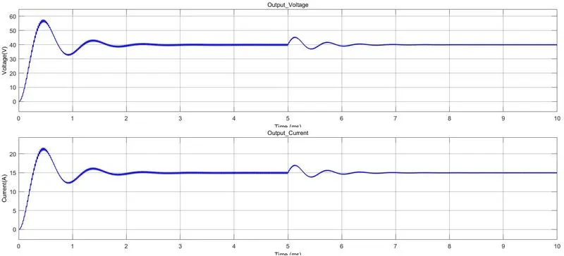
Fig-02: Waveforms of Output voltage and current for Boost converter.
From the above waveforms we can observe the output voltage almost 40 V , due to the internal resistance of the switching devices the output voltage is not exactly 40 V. And at t=5 msec we can observe small overshoot during transient and settles down in the steadystate.
2.Input Voltage and Current waveforms:
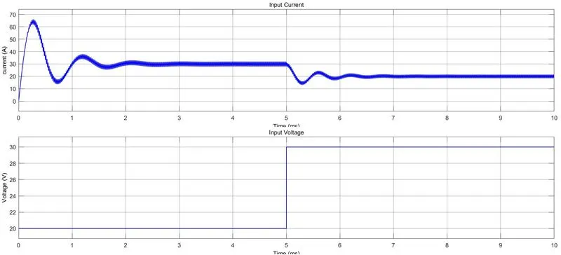
Fig-03: Waveforms of Input voltage and current for Boost converter.
At t=5 msec , the input voltage is varied from 20 to 30 V. Here, the input current is almost DC waveform. Hence, the inductor is acting as the input filter.
3. Inductor current and Duty ratio waveform:
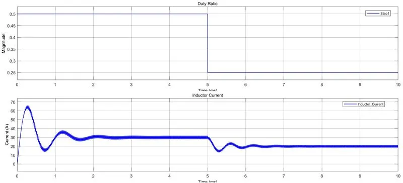
Fig-04: Waveforms of Inductor current and Duty ratio for Boost converter.
According to design requirement the inductor current ripple is maitained below 25% of Average inductor current and it is in Continuous conduction mode(CCM).
4. MOSFET and Diode Voltage waveform:
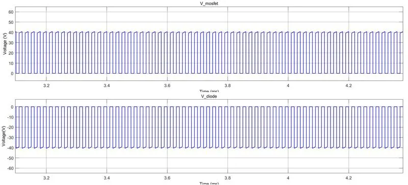
Fig-05: Waveforms of MOSFET and Diode Voltage for Boost converter.
From the above waveforms we can observe that the maximum breakdown voltage of devices. Hence, we can choose the breakdown voltage ratings of swiching devices accordingly. Here, the devices breakdown voltages are same and it doesnot depend on the duty ratio, it depends on the output voltage i.e., 40 V.
3) Sol:- To design the Buck-Boost converter in Continuous Conduction Mode(CCM) using MATLAB(Simulink)
The design reqiurements are as follows:
- Vi= 30-60 V
- Vout= -45 V
- Po= 300 watts
- fs=50 kHz
- `deli_L le 10% of I_L`
- `delv_c le 1%` of `V_o`
For Buck-Boost converter we have , output voltage= Vo=`((D)(V_i))/(1-D)` -----(1)
Load resistance=R=`V_o^2/P_o=45^2/300=6.75`
R=6.75 ohms ------(2)
Output Current=Io=`P_o/V_o=300/(-45)=-6.67`
Io=-6.67 A --------(3)
Determine Duty ratio:
As the input voltage is varying , so does the duty ratio as to vary to maintain the output voltage constant accordingly.
Dmax:
When Vi=30 V ,
using equation(1) `D_max=V_o/(V_o-V_i)=-45/-45-30=0.6`
Dmax=0.6 ----------(4)
Dmin:
When Vi=60 V ,
using equation(1) `D_min=V_o/(V_o-Vi)=-45/-45-60=0.4285`
Dmin=0.4285 ----------(5)
But under steadystate condition the inductor average current =`I_L=(I_o)/(1-D)` ----(6)
Inductor average current(`I_L`):
For Dmax=0.6:
Using equations (3),(4)&(6)
`I_L=(I_o)/(1-D_max)=6.67/(1-0.6)=16.67`
`I_L=16.67 A`---------------(7)
For Dmax=0.4285:
Using equations (3),(5)&(6)
`I_L=(I_o)/(1-D_min)=6.67/(1-0.4285)=11.67`
`I_L=11.67 A`---------------(8)
Now the Ripple inductor current is given by , `delI_L= 10 %`of `I_L` ----------(9)
For Dmax=0.6:
Using equations (7)&(9)
`delI_L= 10/(100)(16.67)`
`delI_L=1.67 A` ----------(10)
For Dmax=0.4285:
Using equations (8)&(9)
`delI_L= 10/(100)(11.67)`
`delI_L=1.167 A` ----------(11)
Capacitor voltage ripple is given by
`delV_c= 1 % of Vo`
`delV_c=1/100(45) = 0.45 V`------------(12)
Inductor design(L):
To maintain the circuit to operate in continuous conduction mode(CCM) , the critical inductance required is given as,
`L_(cr)=((1-D)(V_o))/(f_s*delI_L)` ----------(13)
- For Vi=30 V ,Dmax=0.6 and `delI_L=1.67 A` :
`L_(cr)=(45(1-0.6))/(50e3*1.67)`
`L_(cr)=2.16e-4 H` -----------------------(14)
- For Vi=60 V , Dmin=0.4285 and `delI_L=1.167 A`:
`L_(cr)=(45(1-0.4285))/(50e3*1.167)`
`L_(cr)=4.4e-4 H` -----------------------(15)
Hence , for worst case scenario i.e., to have the continuous current through inductor . The value of inductance is :
L> max{ equation(14), equation(15) }
L> max{ 2.16e-4 H, 4.4e-4 H }
Therefore , let the value of L= 1 milliH -------------(16)
Capacitor Design(C):
The critical capacitance required to maitain the output voltage ripple low as the design requirement.
`C_(cr)=(D)V_o/(R*f_s(delV_c))`
- For Vi=30 V and Dmax=0.6 :
`C_(cr)=(0.6)*45/((6.75)(50e3)(0.45))`
`C_(cr)=2.16e-6 F`-----------------------(17)
- For Vi=60 V and Dmin=0.4285 :
`C_(cr)=(0.4285)*45/((6.75)(50e3)(0.45))`
`C_(cr)=5.7e-6 F`-----------------------(18)
Hence, for maitaining the voltage ripple less than 1% , we need to have a capacitance which is greater the both cases values.
Therefore, C> Max{ equation(17), equation(18) }
C> Max{2.16e-6 F , 5.7e-6 F }
Let, the value of capacitance is C= 10 microF.
Specifications of Boost converter:
- L=1e-3 H
- C=10e-6 F
- R=6.75 ohms
- fs=50 kHz
- Vi=30 - 60 V
- P=300 watts
Simulink model of Boost converter:
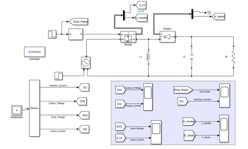
Fig-01: The simulink model for Buck-Boost Converter
As the input voltage is varying the step function is used to vary the input from 30 - 60 V at t=20 msec , same with the duty ratio D= 0.6 to 0.4285 at t=20 msec and generating accordingly the pulses to turn ON and OFF the MOSFET and thus to maintain the output voltage constant at Vo=-45 V.Here, the output voltage is inverting.
Results:
1.Output voltage and current waveforms:
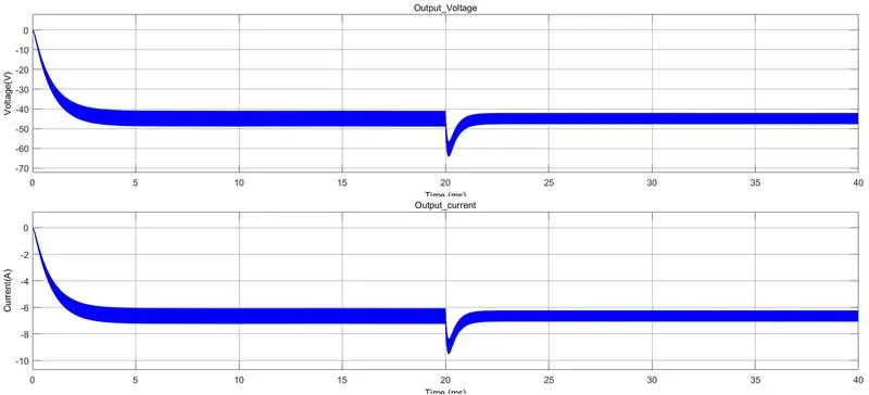
Fig-02: Waveforms of Output voltage and current for Buck-Boost converter.
From the above waveforms we can observe the output voltage almost -45 V , due to the internal resistance of the switching devices the output voltage is not exactly -45 V. And at t=20 msec we can observe small overshoot during transient and settles down in the steadystate.
2.Input Voltage and Current waveforms:
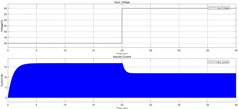
Fig-03: Waveforms of Input voltage and current for Buck-Boost converter.
At t=20 msec , the input voltage is varied from 30 to 60 V.Here, the input current is pulsating DC waveform. Hence, to make input a pure DC value we need to add the input filter.
3. Inductor current and Duty ratio waveform:
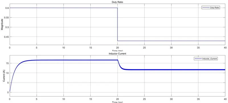
Fig-04: Waveforms of Inductor current and Duty ratio for Buck-Boost converter.
According to design requirement the inductor current ripple is maitained below 10% of Average inductor current and it is in Continuous conduction mode(CCM).
4. MOSFET and Diode Voltage waveform:
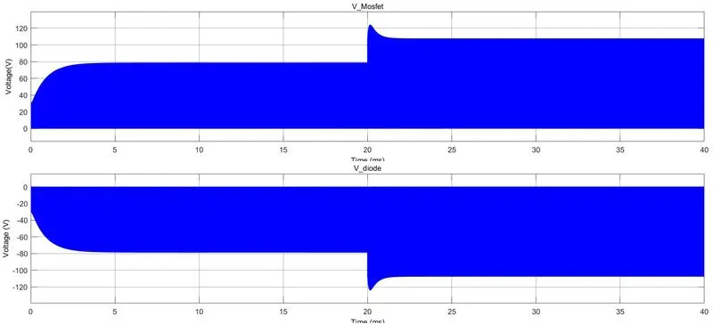
Fig-05: Waveforms of MOSFET and Diode Voltage for Buck-Boost converter.
From the above waveforms we can observe that the maximum breakdown voltage of devices. Hence, we can choose the breakdown voltage ratings of swiching devices accordingly. Here, the devices breakdown voltages are same and it doesnot depend on the duty ratio, it depends on the output voltage i.e., -45 V.