Project 1 - 40-V to 80-V adjustable output voltage boost reference design for LIDAR applications
- How will you decide the layer stack up.
Ans:-
Layer stack-up means the arrangement of the copper layers and the insulating layers before PCB layout design, and these layers form a PCB. The consideration of layer stack-up depends on the technical capabilities of the production and the electrical performance requirements of the PCBs.
40-V to 80-V adjustable output voltage boost circuit.
The circuit might have the following components
1 Input voltage supply. Since it is a boost circuit, input would be less than output.
2. Capacitors.
3. voltage regulator IC
4.Resistors
5. transistor
6. inductors
7. zener diodes
Since it is a small circuit top and bottom layers will be enough. All power connections will be at the top layer followed by ground plane at the bottom layer.
Stack-up Planning the good PCB multilayer stack-up is the most important factor in determining the EMC performance of a product. A well designed layer stack-up not only minimizes the energy it radiates, but can also make circuit relatively immune from external noise sources.
Since it has IC,inductors, we need to keep enough distance between two for avoiding EMI issues.
PCB Stackup Design Example
Many possible PCB stackups may be realized, depending on your implementation of the above tips; however, the following illustration is a good reference example for an 8-layer PCB stackup.
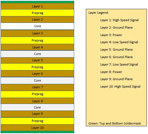
The Above diagram is of Mult layer PCB
When multiple layers are involved, your board design requires you to incorporate a PCB stackup perspective. This perspective is a three-dimensional approach to PCB design where the internal structure is as important as the surface layout.
2) How do you calculate the trace width, via size and trace length?
Ans:-
A PCB trace comprises width, thickness, and length. All these elements affect the functioning of the circuit board. Besides, it is normal to design PCBs with distinct widths based on their intended applications. For instance, traces designed for general applications, such as TTL demand smaller widths than those designed for power transmission
The trace width is basically the width of the copper foil.
The trace width is determined by various factors like current, signal type, temperature, thickness, and others.
One can use many online free software tools that are available to calculate trace width, via size and trace length depending upon the application. Most important factors that decide the trace width,length are the value of current it carries, heat dissipation values, surge curent,overload current,open circuit voltage to avoid arc build up.
The best way of finding the PCB trace width is by applying the trace width equation. The formula will enable you to find the tolerable current conducted through a particular trace. Below is the IPC 2221 trace width formula:
I=k*ΔT^0.44*A^0.725
I is the current, and it is always constant. ΔT is the temperature change, and A is the cross-sectional area.
Longer traces create a high resistance, implying that length is also an important PCB trace resistance consideration. You should aim to design a small board by minimizing the length of the traces.
Trace spacing refers to the distance between two traces. Like the trace width and length, it is also an important trace resistance consideration. Importantly, trace spacing will enable you to prevent flashovers between two conductors. A flashover is a current breakdown that appears along the PCB surface or junction.
The trace resistance of a microstrip is important in determining how much power it dissipates. By determining its trace resistance, the contribution of a microstrip to the overall circuit resistance can be evaluated. This tool is designed to calculate the resistance of a microstrip trace with a copper conductor. To use it, specify the trace dimensions and the ambient temperature.
Equation
Where:
ρ=resistivity
L= length
W=trace width
T=trace height
3.What is the drawback of having 2 layers PCB?
Ans:-
- Simplistic Design – A 2-layer PCB typically has a simple design and has less room for more components and routing options.
- Slower Speed and Lower Operating Capacity – If speed is an issue, the more layers, the better. Depending on the application, you may find that 2 layers isn’t enough to give you the necessary speed and capacity for your project.
- Larger Size and Higher Weight – Double sided PCBs are typically quite large and bulky in comparison to make room for components and leads. If you need to fit your printed circuit board into a compact space, adding more layers is often the best design choice.
- Using 2-layer boards for these kinds of circuits would not only cause emission of excessive amounts of radiation and interference, but signal integrity would also be compromised.
- These circuits are too simplistic for complex projects.
- Single-sided boards have a lower operating capacity.
- Moreover, they are larger in size.
- Due to a larger size, these have a higher weight.