Project 1 - 40-V to 80-V adjustable output voltage boost reference design for LIDAR applications
- How will you decide the layer stack up.
The PCB Stackup Design Perspective
Regardless of the number of layers that comprise your board design, specifications for pad spacing, clearances, trace widths, copper weights and drill hole sizes must be tailored to your contract manufacturer (CM). If your design requires multiple layers, you will need to consider additional design for manufacturing (DFM) specifications for signal, power and ground routing through vias, as well as the PCB stackup. These additions entail incorporating verticality into your design perspective.
The PCB stackup design perspective that includes both vertical and horizontal considerations is a three-dimensional approach that significantly impacts board fabrication and PCB assembly. For fabrication, the number of layers, their arrangement or stackup and type of material must be determined. These choices require coordination between thicknesses restrictions; material parameters; such as dielectric constant, the coefficient of thermal expansion and electrical strength, signal type isolation and drill hole options. For PCB assembly, via routing options and their effect on the soldering process are of great importance. The capabilities of your CM limit the choices for the vertical aspect of your design.
Now, we can look at the best ways to implement the PCB stackup design perspective.
PCB Stackup Design
Determining the number of layers
The first consideration for your PCB stackup is determining how many layers are needed. This includes considering signal (high speed, low speed), power (for high power boards or when power supplies are a part of your circuit) and ground layers or planes. It is highly recommended not to mix signal types on inner layers. For most boards, you can use the pin density to get an accurate layer count:
After calculating the pin density, you may use a readily available lookup table to find the number of signal layers and total layers or consult your CM for stackup support. You may be required to furnish additional information, such as control impedance values.
Determining the layer arrangement
After determining the number the layers, you need to determine how they should be arranged or stacked. Good rules to follow here are:
- Route high-speed on minimum thickness microstrips.
- Place signal layers next to internal power layers for tight coupling.
- Power and ground layers should have minimal spacing between them.
- Avoid having two signal layers adjacent to each other.
- Make the stackup symmetric from the top and bottom layers inward.
Determining layer material types
An important consideration for your PCB stackup is the thickness of each signal layer. This should be established in conjunction with determining thicknesses for prepreg and core(s). There are standard thicknesses, as well as other properties, for different circuit board material types. Your process for selecting materials should include these electrical, mechanical and thermal properties.
Determining routing and vias
Completing the PCB stackup design is the determination and routing of the traces. This includes determining copper weights, where to put vias and what type of vias to implement. As for all specifications for your design, you should work with your CM in making these determinations as some CMs avoid certain via types, such as via-in-pads.
PCB Stackup Design Example
Many possible PCB stackups may be realized, depending on your implementation of the above tips; however, the following illustration is a good reference example for an 8-layer PCB stackup.
Example 10-layer PCB stackup
When multiple layers are involved, your board design requires you to incorporate a PCB stackup perspective. This perspective is a three-dimensional approach to PCB design where the internal structure is as important as the surface layout. By applying the tips above, you can easily overcome the nuances associated with this design approach and including your CM from day 1 of design should ensure that your PCB stackup is the best manufacturable implementation for your requirements that meet your CM’s capabilities.
in basic 2layer 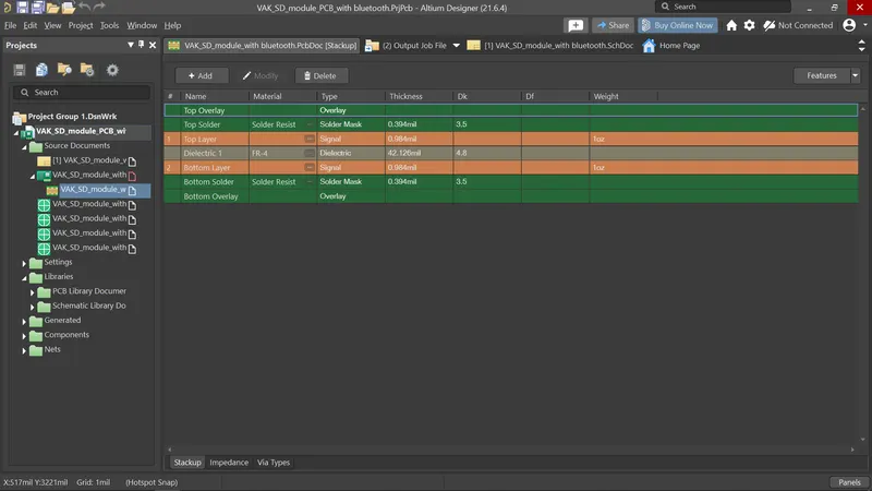
for 4layer
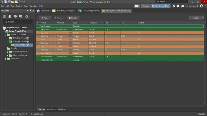
2.How do you calculate the trace width, via size and trace length.
How is PCB Trace Width Calculated?
Let's walk through the process of calculating for a certain trace width for a power signal delivering current from one power component to a peripheral. In this example, we’ll be calculating the minimum trace width for a power-path used for a DC motor. The power-path starts at a fuse, travels through an H-bridge (a component used to manage power delivery across a DC’s motor windings), and ends at the motor’s connector. The average continuous max current demanded by the DC motor will be around 2 Amps.
Now, a PCB trace acts as a resistor and the longer and narrower the trace, the more resistance is added. If the trace isn’t properly defined, the high current could damage the trace and/or introduce significant voltage drop to the motor (resulting in a slower speed). NetC21_2 shown in Figure 3 is about 0.8” long and needs to carry 2 Amps max. If we assume some general things like a 1-ounce copper pour and ambient room-temperature during normal operation, we have what we need to calculate both the minimum trace width and expected voltage drop at that width.
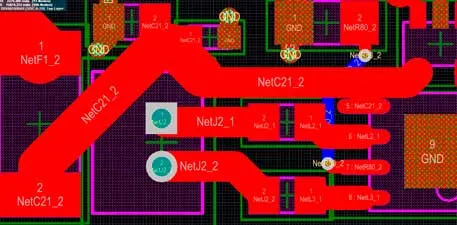
Example of optimized trace width for DC motor's power-path
How do you Calculate PCB Trace Resistance?
The following is an equation used for trace area:
Area[mils²] = ( Current[Amps] / (k*( Temp_Rise[°C] )^b) )^(1/c) where following IPC guidelines for an external (or top/bottom) layer, k = 0.048, b = 0.44, c = 0.725. Note that the only variable we really need to plug in here is current.
And using this area in the following equation will give us the necessary width which tells us how wide our trace needs to be to carry the current without any potential issues:
Width[mils] = Area[mils^2]/(Thickness[oz]*1.378[mils/oz]) where 1.378 is associated with the standard 1 ounce pour thickness.
By plugging in 2 amps into the above calculation we get around 30 mils minimum for the trace.
But what this doesn’t tell us is what the voltage drop will be. This is a bit more involved as it requires a calculation of the trace’s resistance which can be calculated per the equation shown in Figure 4.

Figure 4. Formula for PCB trace resistance
In this formula, ρ = resistivity of copper, α = temperature coefficient of copper, T = trace thickness, W = trace width, L = trace length, and t = temperature. If all the associated values are plugged in for a 0.8inch long trace at 30mils width, we find that the trace resistance will be around 0.03? and will drop the voltage about 26mV which would be more than OK for the application. It’s helpful to know what impacts these values.
PCB Trace Spacing & Length
For digital designs with high speed communication, specific spacing and tuned lengths may be required to minimize cross-talk, coupling, and reflections. Some common applications for this are USB-based serial differential signals, and RAM-based parallel differential signals. Generally, USB 2.0 will require differential pair routing at speeds of 480Mbit/s (USB high speed class) or higher. This is partly because high-speed USB generally operates at a much lower voltage and differential, bringing the overall signal level closer to the noise floor.
There are three important things to consider when routing high speed USB lines: trace width, trace spacing, and trace length.
All are important but the most critical out of the three is making sure the two traces are matched as closely as possible in length. As a general rule of thumb, if the traces differ any more than 50 mils in length from each other (for high speed USB), it significantly increases risk of reflections which could result in poor communication. 90 Ohm matched impedance is a common specification for differential pair routing and to achieve this, the traces should be optimized in width and spacing.
Figure 5 shows an example of a differential pair routed for a high-speed USB interface, containing 12-mil wide traces at 15-mil spacing.
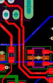
Figure 5. Differential routing for USB2.0 high speed
An interface for a memory-based component containing a parallel interface, such as DDR3-SDRAM, will be much more tightly constrained in terms of trace length. Most higher-end PCB design software will have length-tuning features that will optimize trace length to match all associated signals in a parallel bus. Figure 6 shows an example of a DDR3 layout with length-tuned traces.

Figure 6. Example of length-tuned DDR3 memory traces
Ground-Filled Traces and Planes
Some applications with noise-sensitive components such as wireless chips or antennas may require a little extra protection. Designing traces and planes with embedded ground vias can greatly help minimize coupling picked up by nearby traces or planes and also off-board signals that creep into the board edge.
Figure 7 shows an example of a Bluetooth module placed near the edge of a board with its antenna (labelled via silkscreen “ANT”) on the outside of a thick trace containing embedded vias connected to a ground plane. This helps isolate the antenna from the other on-board circuitry and planes.
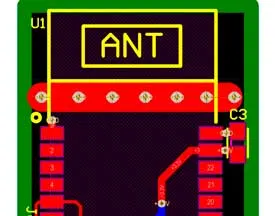
Figure 7. Bluetooth module with a ground-via embedded trace to help with noise suppression
Another method of this ground-via embedded trace (or polygon plane in this instance) could be used to protect the boards circuitry from outside, off-board wireless signals. Figure 8 shows a noise-sensitive PCB with a ground-via embedded plane along the perimeter of the board.
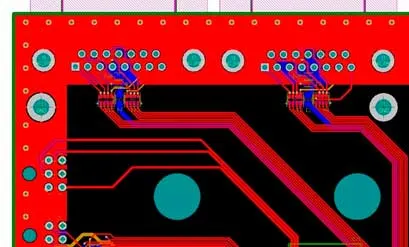
Figure 8. Ground plane with vias lining a sensitive PCB to protect against off-board interference
Best-Practices for PCB Routing
Many things drive trace characteristics in the PCB world so make sure to follow best practices when routing your next PCB and you’ll find that balance between PCB fab cost, circuit density, and overall performance.
If you’re looking for a quote for your next PCB application, connect with our team of experts to help you get exactly what you need at the right price. We specialize in PCB fabrication and PCB assembly conforming to intricate designs typical boardhouses can't manufacture or assemble.
Let us help you bring your design into reality.
3. What is the drawback of having 2 layers PCB?
-Firstly, they are more expensive to manufacture than single-sided boards. -In addition, they require more solder mask layers and thus have a longer manufacturing production process. -Also, the through-hole vias can be difficult to solder.