Project 1
1. Cuk converter
Given,
Vin = 300-600V
Vout = -450V
power= 5Kw
Input voltage considered is 500V
Fs =100KHz
1) Duty cycle
Vo/Vin = -D / (1-D)
D = 0.47
2) Inductor design,
iL1 = P/Vin = 10A, iL2 = P /V0 = 11.11A
R = vo^2 / P = 40.5 ohm
For 10% ripple,
DeltaiL1 = 1A, DeltaiL2 = 1.1A
L1 = (vinD)/ (fs*DeltaiL1) = 2.35mH, L2 = 2.14mH
C1 = V0*D / R*fs*deltaVc1 = 0.549uF
Cout = (1-D) / 8*L2*fs^2*DeltaV0/V0 = 0.309uF
Cuk converter Schematic
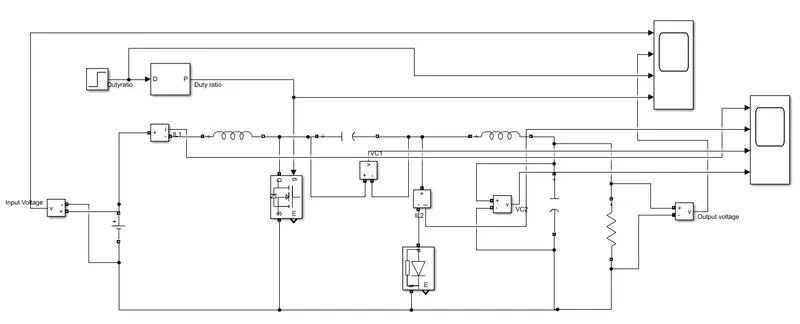
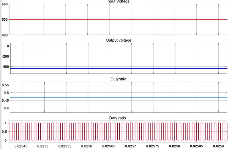
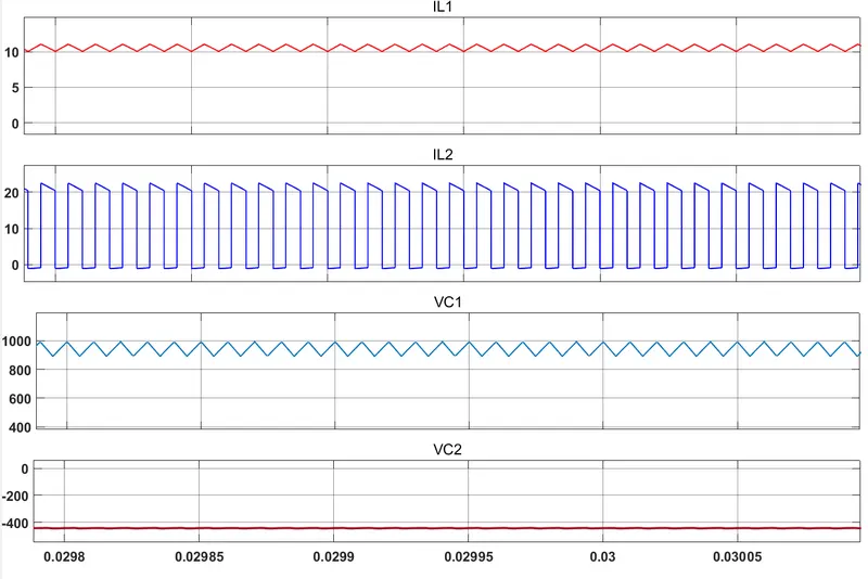
The input and output voltages, duty ratio, current through inductors 1 and 2, voltage across the capacitors are shown in the above waveforms. The output of the Cuk converter for the input voltage of 500V is -450V.
2. Sepic Converter
Schematic
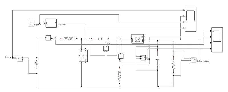
Design,
Vin= 400V, Vout = 450V, P = 6000W
Duty cycle,
Vo/Vin = D/ (1-D)
D= 0.53
R = Vo^2/P = 33.75 ohm
fs =100KHz
Inductor design,
L1 = (vin *D/fs*deltaIL1) = 1.41mH
L2 = (vin *D/fs*deltaIL2) = 1.593mH
C1 = V0*D / R*fs*deltaVc1 = 0.14uF
Cout = D / R*fs*deltaV0/V0) = 0.157uF
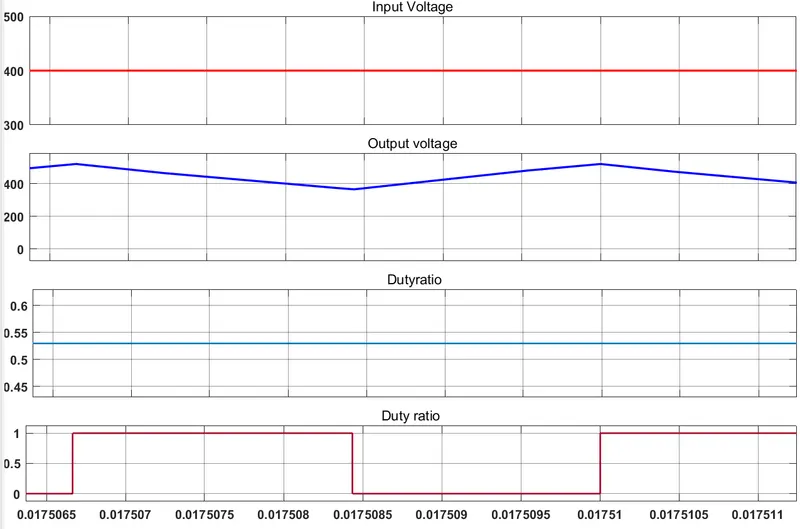
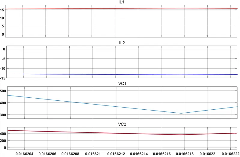
The input and output voltages, duty ratio, current through inductors 1 and 2, voltage across the capacitors are shown in the above waveforms. The input voltage is 400V and the output voltage is 450V. The output voltage across the Sepic converter is positive.
3. Boost Converter
Schematic
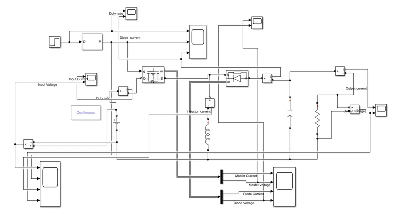
Design,
Vin = 300, vout= 450V, P= 2000W, fs =100KHz
R = Vout^/P = 101.25 ohm
Duty cycle,
Vo/Vin = -D/ (1-D) = 0.6
L = (Vout*(1-D) /fs* deltaIL) = 1.62mH
C = D / (r *fs* deltaV0/V0i)= 5.925uF
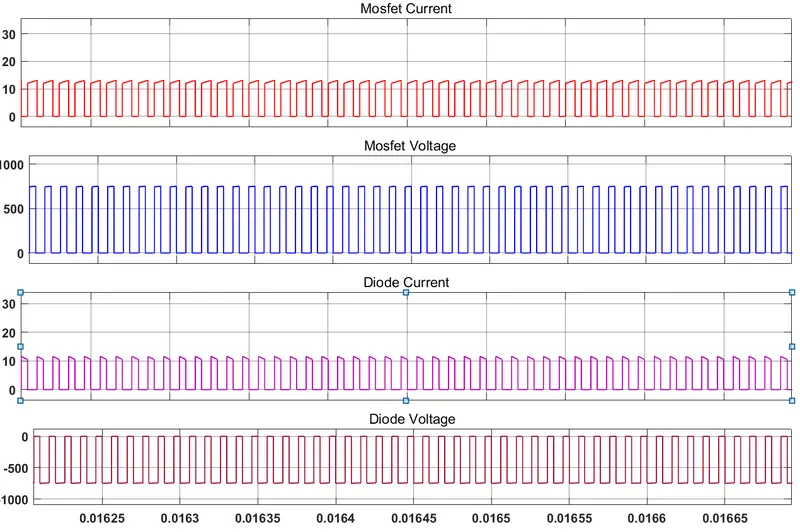
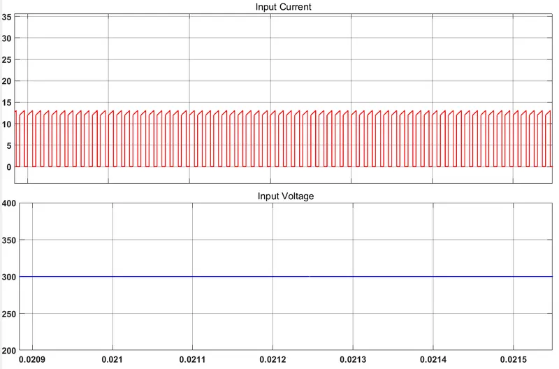
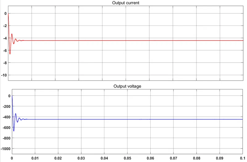
The Mosfet and diode, voltage and current, Input voltage and current, Output voltage and current waveforms are shown in the above waveforms
The input voltage to the converter is 300V and the output voltage from the converter is 450 V. The voltage is boosted up with a negative polarity in the buck boost converter.