Week 6 Challenge: Power Converters
Week 6 Challenge: Power Converters
- Why does MATLAB PID auto tuner doesn’t work for a power converter? Show step wise process for a buck-boost converter circuit.
- Explain the importance of ADC and DAC blocks in closed loop control of power converter.
- Prepare an organizational chart of people working at electric powertrain manufacturing company.
- Why does MATLAB PID auto tuner doesn’t work for a power converter? Show step wise process for a buck-boost converter circuit.
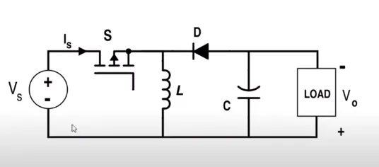
PID Tuner needs a linear model to design a PID controller. To get this linear model, when you press the "tune" button, it automatically linearizes a Simulink model using exact linearization method. This method results in zero linearization when a model has discontinuities such as MOSFET blocks and PWM logic.
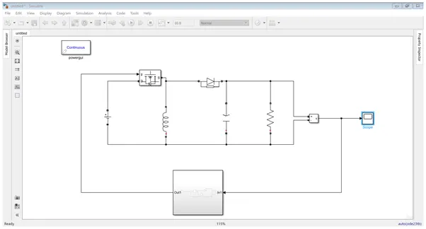
The result of this will be that when you simulate the model, you use your SimPowerSystems blocks with all MOSFETS, PWMs, etc., but when you do linear analysis of the model or PID Tuning, the converter subsystem is replaced with a transfer function automatically.
PID auto tuner can only work for the plants which are linearized or which can be linearized. To work with the auto tuner, the MATLAB first linearizes the plant & then finds the PID gain values but in the case of power converter, it results in zero linearization because of the discontinuities such as MOSFET blocks & PWM logic & hence it cannot auto tune PID.
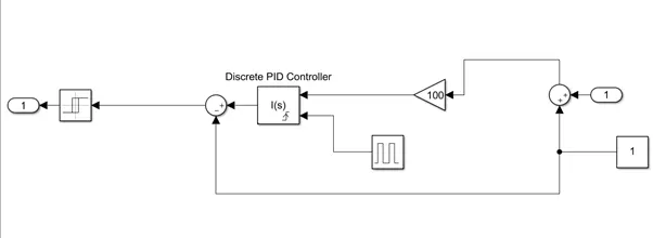
To solve this issue use simulation input/output data to estimate a transfer function of the system and then tune the response.
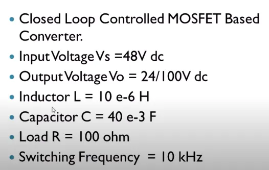
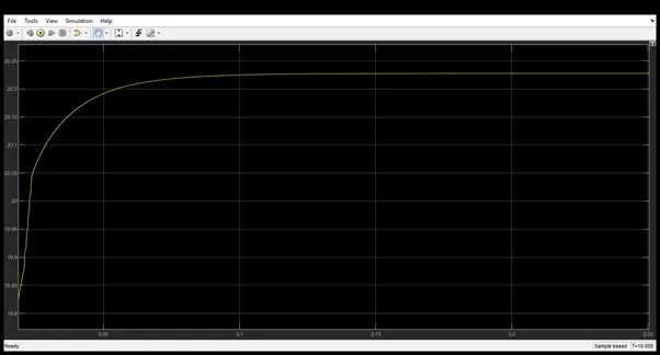
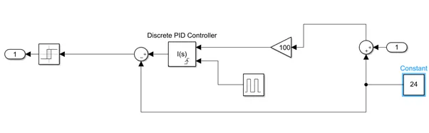
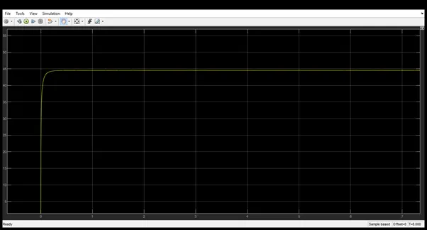
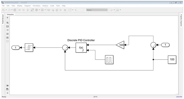
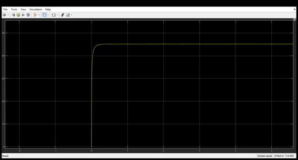
Let’s consider a boost converter which is set to fluctuate the output voltage between 50 to 55 with a closed loop PI converter
- Explain the importance of ADC and DAC blocks in closed loop control of power converter.
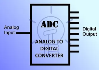
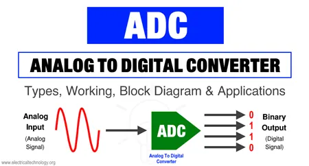
ADC stands for analog to digital converter. It is an electronic device used for converting an analog signal into a digital signal.
The analog input signal of ADC is continuous time & continuous amplitude signal. The output of ADC is a discrete time and discrete amplitude digital signal.
Why ADC?
In the real world, every real quantity such as voice, temperature, weight etc exists in the analog state. And it cannot be processed by any digital device such as a computer or a cell phone.
These analog quantities are converted into digital form so that a digital device can process it. This conversion is done using analog to digital converter.
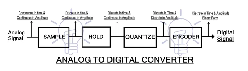
The analog signal is first applied to the ‘sample’ block where it is sampled at a specific sampling frequency. The sample amplitude value is maintained and held in the ‘hold’ block. It is an analog value. The hold sample is quantized into discrete value by the ‘quantize’ block. At last, the 'Encoder' converts the discrete amplitude into a binary number.
Analog to Digital Conversion Steps -
The conversion from analog signal to a digital signal in an analog to digital converter is explained below using the block diagram given above.
Sample
The sample block function is to sample the input analog signal at a specific time interval. The samples are taken in continuous amplitude & possess real value but they are discrete with respect to time.
The sampling frequency plays important role in the conversion. So it is maintained at a specific rate. The sampling rate is set according to the requirement of the system.
Hold
The second block used in ADC is the ‘Hold’ block. It has no function. It only holds the sample amplitude until the next sample is taken. The hold value remains unchanged till the next sample.
Quantize
This block is used for quantization. It converts the analog or continuous amplitude into discrete amplitude.
The on hold continuous amplitude value in hold block goes through ‘quantize’ block & becomes discrete in amplitude. The signal is now in digital form as it has discrete time & discrete amplitude.
Encoder
The encoder block converts the digital signal into binary form i.e. into bits.
As we know that the digital devices operate on binary signals so it is necessary to convert the digital signal into the binary form using the Encoder.
This is the whole process of converting an Analog signal into digital form using an Analog to Digital Converter. This whole conversion occurs in a microsecond.
Factors Of ADC
Resolution:
Resolution of an ADC is the number of bits that represents the digital signal’s amplitude.
The analog signal has continuous amplitude. It can have infinite values i.e. real, floating basically any value one can imagine. On the other hand, the digital signal has a discrete and finite number of values. These discrete values are represented using binary numbers (bits).
To better understand the idea of resolution of ADC,
- 1-Bit Resolution
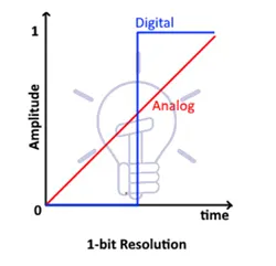
The figure above shows an analog signal represented in a digital form which is either 0 or 1. This is a 1-bit resolution. The resolution of ADC defines its number of steps.
number of steps = 2n
Where n is the number of bits. Therefore, there are 2 steps in 1-bit resolution.
- 2-Bit Resolution
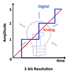
This figure shows the conversion of analog to digital in 2-bit resolution. There are 4 steps or quantization levels.
No of steps = 2n = 22 = 4
- 4-Bit Resolution
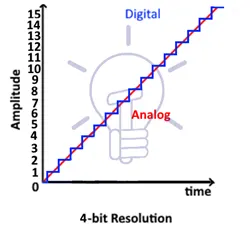
This figure shows 4-bit resolution. The number of steps in 4-bit resolution is 16.
No of steps = 2n = 24 = 16
The number of steps increases exponentially with increase in the bit-resolution. It also implies that by increasing the bits of resolution the converted digital signal becomes more like the original analog signal. So ideally, we can say that a digital signal with infinite resolution is an analog signal.
Width Of The Step
The voltage difference between two adjacent steps is known as the width of the step. It is denoted by Δv.
So a single step represents a fixed voltage that is
Δv = vref/2n
Where vref is the maximum voltage being converted & n represents the bits of resolution.
For example:
vref = 10.24v & n = 10 bits
Then:
Δv = 10.24/210
Δv = 10.24/1024
Δv = 0.01v
Thus the step-size or width of the step is 0.01v. In this ADC, a single bit increase represents a 0.01v of increase in the analog input. If analog input is increased by 0.01v then the output is increased by 1 bit.
Quantization Error
The ADC updates its value if the increase or decrease in its input voltage is greater than Δv/2. Any change less than Δv/2 will not be registered. This is known as Quantization Error.
In other words, the difference between the input and the digital round-off figure of output is known as quantization error.
The increase in the resolution of the ADC decreases the step-size if the vref remain constant. Consequently, the quantization error decreases.
Sampling Rate
The number of samples taken during a single second is known as sampling rate or sampling frequency.
The sampling rate should be set according to the input signal. It should not be very low or very high.
Example of sampling:
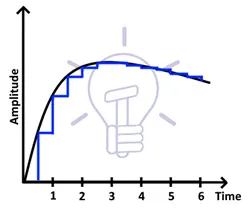
This example shows that the sampling rate is 0.5 sec, as it takes 2 samples in one second.
Aliasing
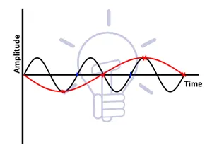
If the sampling rate is very low then the resultant signal will not look anything like the original signal. In fact, it will become a different signal after reconstruction. This problem is known as aliasing.
To avoid this problem, the sampling rate should be kept higher than twice the frequency of the input signal. Anti-aliasing filters are also used for removing the frequency components higher than one half of the sampling rate. it blocks the aliasing components from being sampled.
Nyquist Criteria
Nyquist criteria suggest the minimum possible sampling rate for an analog signal which can be reconstructed successfully. If the highest frequency of the analog signal is f, the signal can be reconstructed successfully from its samples, if the samples are taken at a sampling frequency greater than 2f.
Offset
The offset in ADC is the shift in the digital output. For example, for input vin = 0, the output might not necessarily be digital 0. It can be digital 5, which will be the offset of the ADC.
Application of ADC
In the modern world of growing technology, we are dependent on digital devices. These digital devices operate on the digital signal. But not every quantity is in digital form instead they are in analog form. So an ADC is used for converting analog signals into digital signals. The applications of ADC are limitless. Some of these applications given below:
- Cell phonesoperate on the digital voice signal. Originally the voice is in analog form, which is converted through ADC before feeding to the cell phone transmitter.
- Imagesand videos captured using camera is stored in any digital device, is also converted into digital form using ADC.
- Medical Imaging like x-ray& MRI also uses ADC to convert images into Digital form before modification. They are then modified for better understanding.
- Music from the cassetteis also converted into the digital form such as CDs and thumb drives using ADC
- Digital Oscilloscopealso contains ADC for converting Analog signal into a digital signal for display purposes & different other features.
- Air conditionercontains temperature sensors for maintaining the room temperature. This temperature is converted into digital form using ADC so that on-board controller can read & adjust the cooling effect.
In today’s modern world almost every device has become the digital version of itself & they need to have ADC in it. Because it has to operate in digital domain which can be only acquired using analog to digital converter (ADC).
The accuracy of a control system depends on how predictable the load is, the control architecture selected, and the precision of the components executing control. The following overview provides tips on selecting digital-to-analog converters for various control-loop applications.
When it comes to selecting a Digital-to-Analog Converter (DAC), designers can choose from a wide range of ICs. DACs can be divided into many different categories for specific applications. The field can be narrowed by differentiating between those needed for DC or low-speed adjustments versus those needed for high-speed waveform generation. This article focuses on those needed for low-speed applications, whether low resolution or high resolution or coarse or fine adjustment.
In terms of selecting a low-speed DAC, it is important to determine whether the design is a closed-loop, open-loop, or “set and forget” system. Each of these will require a DAC with key specifications.
Closed-loop systems include a feedback path to sense and correct for any errors. A sensor monitors the output from a physical parameter such as a servo motor, flow valve, or temperature-sensing element. The sensor then feeds the data back to a controller, which uses this information to determine if a correction is necessary.
DACs and Analog-to-Digital Converters (ADCs) are key components at the heart of a closed-loop system. While a DAC is used in the feed-forward path to make adjustments to the system, an ADC is used in the feedback path to monitor the effect of those adjustments. Together, they force and sense the analog control signals to make real-world adjustments to the parameter they’re controlling.
Motor control is one example of a closed-loop system, as detailed in Figure 1. First, a desired output (set point) is applied to the controller, which compares this to the feedback signal. If a correction is required, the controller will adjust the input code to the DAC, which then produces an analog voltage at its output. The DAC output voltage is amplified through a power amplifier to provide the required drive current to the motor.
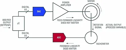
A closed-loop system’s performance depends on an accurate feedback path, including the sensor and ADC. In essence, the feedback path compensates for errors in the feed-forward path. Because the DAC is in the feed-forward path, its Integral Non-Linearity (INL) error is automatically compensated for. INL error is the deviation of the actual transfer function at the DAC output from the ideal transfer function.At the next stage of this closed-loop system, a tachometer is used to measure the rotational speed of the motor. The rotation signal is the actual output, or process variable, of the closed-loop system. An ADC digitizes the tachometer’s output and sends the data to the controller, where an algorithm determines if any correction needs to be made at the DAC output, and ultimately, the motor. In this way, the error is reduced to an acceptable level. Feedback ideally allows the closed-loop system to cancel out all errors, effectively limiting the effects from any errant sources of noise, temperature, force, or other unwanted signals.
The DAC must have adequate Differential Non- Linearity (DNL) and be monotonic to the number of bits specified in the data sheet. DNL error is the difference between the actual voltage change at the DAC analog output versus an ideal voltage step equal to a 1 Least Significant Bit (LSB) step in the DAC input code. A monotonic DAC means the analog output always increases or stays the same with an increase in the digital code (and vice versa). A DNL spec that is always greater than -1 LSB implies monotonicity. Figure 2 shows the transfer function of DAC analog output voltage versus DAC input code.
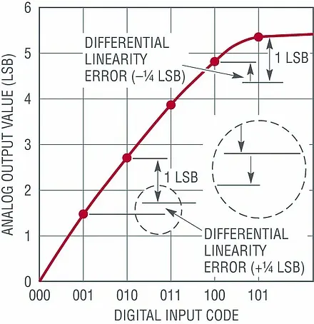
If the DAC is not monotonic, there will be a region where negative feedback turns into positive feedback. This can lead to oscillation that could eventually destroy the motor.
Open-loop systems do not have a feedback path. This means the system must be accurate on its own. Open-loop control is useful for well-defined systems where the relationship between the input code and the resulting action on the load is known. If the load is not very predictable, it’s best to use closed-loop control.
An example of an open-loop system is shown in Figure 3. In this example, the DAC drives the SET voltage pin of linear regulator LT3080. The SET pin is the input to the error amplifier and the regulation set point for the output voltage. The LT3080’s output voltage range is from 0 V to the absolute maximum rated output voltage.
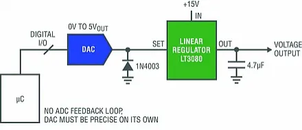
Other important parameters in an open-loop system are offset, gain error, error of the reference voltage, and the stability of these parameters over time and temperature. INL is of particular importance because in contrast to the closed-loop system, the INL of the DAC has a direct bearing on the overall linearity of the system.The resolution of the DAC determines the step size for adjustments to the SET pin. For example, an 8-bit DAC with a 5 V reference has an LSB size of 5 V/28 = 19.5 mV. A 12-bit DAC with the same 5 V reference has an LSB size of 1.2 mV, and a 16-bit DAC has an LSB size of 76 mV. This means that for an ideal DAC, every increase in the digital code should increase the analog output 76 mV.
A third application where DAC linearity plays an important role is set and forget systems. In these systems, an adjustment or calibration is made once, perhaps at the time of manufacture or during installation. This system starts life as a closed-loop system and then goes open loop. Thus, any parameter related to initial accuracy (offset, gain error, INL) is not critical, as it is compensated for during the adjustment. But once the feedback is removed, stability becomes key. Data sheet specifications that indicate stability are gain error drift, offset drift, and reference drift.
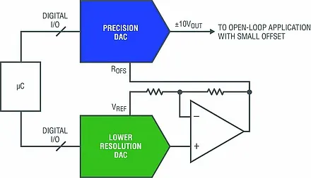
Figure 4 shows an example of a set and forget application. In this figure, a lower-resolution DAC drives an amplifier that sets the voltage at an offset adjustment pin for a precision DAC. The lower-resolution DAC is used to effectively calibrate the gain offset out of the precision DAC during initial system calibration. This adjustment code can be stored in nonvolatile memory and loaded each time the system is powered up.
When the output from the power converter is coming out it is also fed into the digital controller (Closed Loop Control) but an ADC block is required to eliminate the signal nature difference between both the components similarly when the output from the controller goes to the power converter it is of digital nature & needs to be converted into continuous signal hence a DAC is required.Also, in real world applications all the signals are continuous so when the power converter is used the input control signal as well as the output of the power converter are continuous signals, but while designing a controller for a microprocessor the control has to be in the digital domain so that it can be implemented this creates a difference between the signal nature and to eliminate this difference ADC or DAC blocks are used.
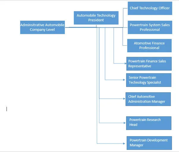
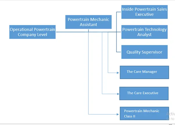
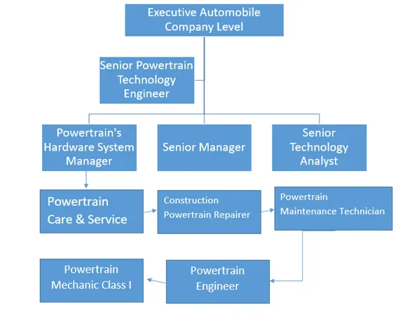
3. Prepare an organizational chart of people working at electric powertrain manufacturing company.
Also known as an org chart or organogram, it provides a detailed visual representation of an organization, key individuals, teams, and the relationship between them. These charts are mostly related to established firms, government sectors, or huge organizations with a complex hierarchy. Ideally, there can be all kinds of org charts, depending on their application and usability.
Mostly, it acts as a useful tool for human resource professionals and corporate analysts. They can easily represent the overall breakdown of an organization, its workload, and identify the key individuals responsible for certain tasks. For instance, you can consider this organizational chart that represents the hierarchical employment flow in a firm.
It might sound surprising, but organizational charts have been a part of engineering and management sector for over a century now. The concept was first introduced in 1854 by Daniel McCallum, who was an experienced engineer. While the concept was introduced by McCallum, the first chart was drawn by George Holt Henshaw.
Shortly, all the essential guidelines and theory about the chart was also listed. Though, it took a while for organizational charts to become mainstream. Even till 1920, the concept was not fairly known by professionals. By the same time, Brinton focused on the wide application of the charts and came up with numerous examples to show their applications.
Gradually, they found a way in business and administrative work. In the 1960s, they were known as “organigram” or “organogram”. Today, they have become an evident part of daily professional work in every major organization.
- Divvesh MadaswarDesign a boost converter that will have an output of 30 V from a 12 V source. Take ripple current of 3% and an output ripple voltage of less than one percent. Take a resistance of 50Ω. Assume ideal components for this design. please challenge answer