Project 2
OBJECTIVE
Design an interleaving DC/DC converter system for a data centre application with the following specifications:
- Input voltage: 45 – 60 v
• Output voltage: 3 V
• Output current: 100A
• Efficiency > 85% (extra credit for efficiency higher than 90% on a spice-based software simulation tool)
Simulate the system using a Spice-based software simulation tool such as LT-Spice, Pspice, PowerSim, TINA, etc...
Show your design in details (most probably, you will need to use an isolated system to achieve this low voltage conversion ratio, you might also need to use a multiphase system to increase the efficiency).
Show the input voltage, the output voltage, the input current, the output current, the system efficiency and any other simulation plots necessary to evaluate your design.
SOL)
The interleaved technique can be used to step down a high DC voltage to very low DC voltage with lesser voltage ripple and low value of inductor and capacitor thus reducing the size. With conventional buck chopper for converting high voltage to low voltage, very small duty cycle is required which further adds several limitations on different components and triggering circuitry and requires relatively high values of inductor and capacitor to insure permissible current ripple and voltage ripple i.e. within limits
The electrical power is growing at a rapid rate and to meet this demand, more efficient systems and low power applications play a vital role .In order to fulfill the increasing demand, faster and most efficient devices such as data processor, microprocessors, portable devices efficient system are required. The continuous sandwiching the large number of devices on single chip has increased the current demand with good power quality and extremely low margin of tolerance i.e. voltage ripple and current ripple .The proposed interleaved dc-dc converter gives low voltage and high current at its output. Since interleaving methodology is used to minimize the voltage ripple at the output terminals
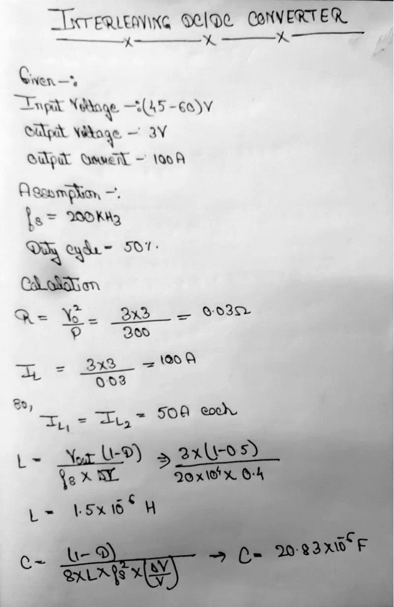
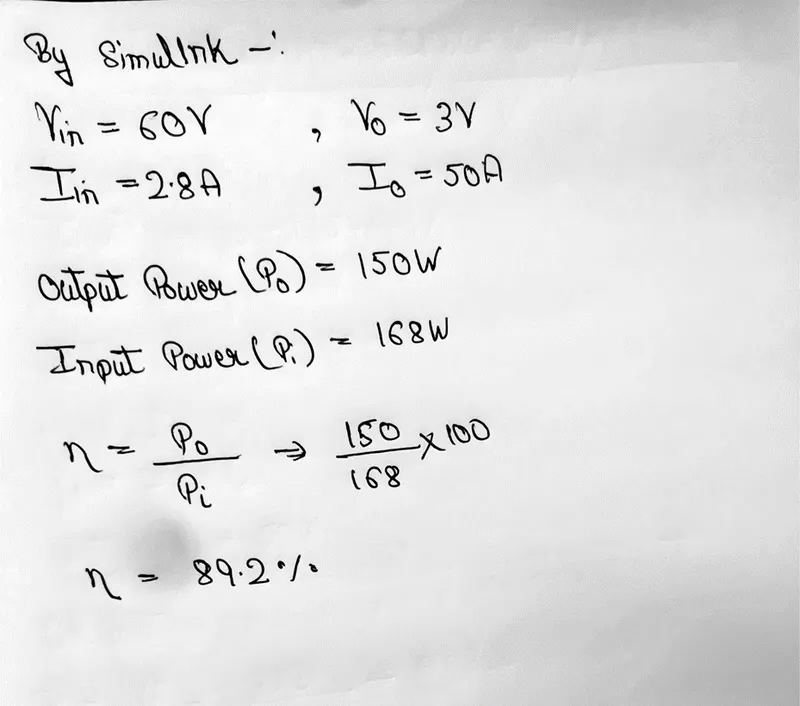
CALCULATION:
BLOCK DIAGRAM
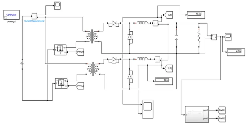
COMPONENT USED IN CONVERTER:
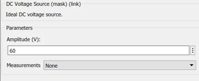
- INPUT SOURCE:
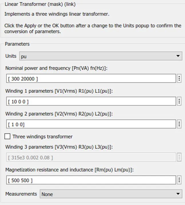
- TRANSFORMER
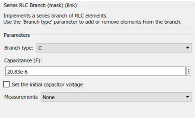
- CAPACITANCE
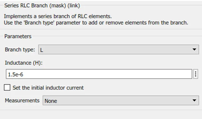
- INDUCTANCE
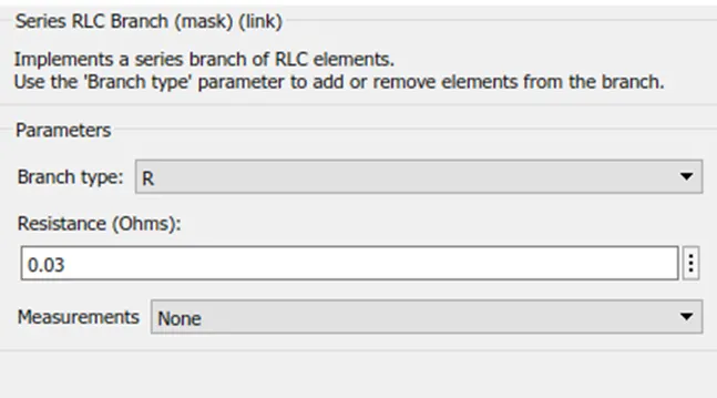
- RESISTANCE
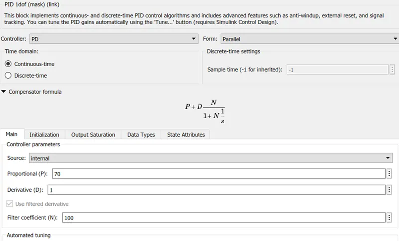
- PID CONTROLLER
- TRIANGULAR WAVE
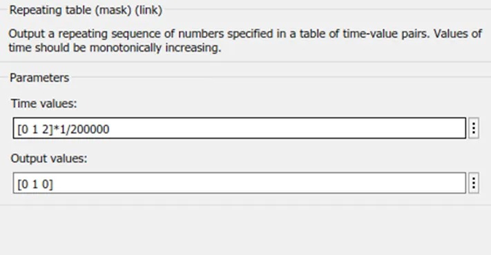
Here the frequency is choose as 200kHz
GATE DRIVER
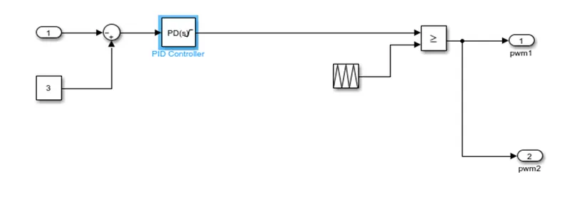
The output waveform is compare to reference wave and the error is goes to PID controller which is then compare to relational operator and then given to MOSFET 1 and 2
OUTPUT WAVEFORM
- OUTPUT VOLTAGE
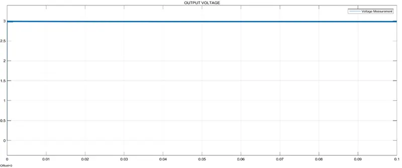
The output voltage is 3V with very small ripple approx. 1%
- INDUCTOR CURRRENT
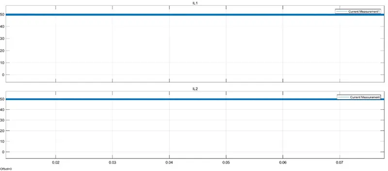
The inductor current(IL1 & IL2) low which is 50A So, we get less losses ,less ripple current and high efficiency
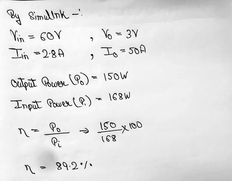
In the above calculation we get efficiency greater than 85%
Conclusion:
Those we designed the DC/DC converter the given data and get the required output with more than 89.2% efficiency.